Semiconductor device, power circuit, and manufacturing mkethod of semiconductor device

a semiconductor and power circuit technology, applied in the field of semiconductor devices, can solve the problems of difficult melting of silicon carbide, inability to manufacture silicon carbide by a high-productivity method, and defects called micropipes, and achieve high breakdown voltage, high conversion efficiency, and high-speed switching

Inactive Publication Date: 2011-03-24
SEMICON ENERGY LAB CO LTD
View PDF99 Cites 54 Cited by
  • Summary
  • Abstract
  • Description
  • Claims
  • Application Information

AI Technical Summary

Benefits of technology

[0019]A semiconductor device for high power application such as a power MOSFET needs to have characteristics such as high breakdown voltage, high conversion efficiency, and high-speed switching. Nowadays, silic

Problems solved by technology

However, it is difficult to melt silicon carbide because of its characteristics; therefore, silicon carbide cannot be manufactured by a method having high productivity such as a Czochralski (CZ) method or the like which is used

Method used


Image

  • Semiconductor device, power circuit, and manufacturing mkethod of semiconductor device
  • Semiconductor device, power circuit, and manufacturing mkethod of semiconductor device
  • Semiconductor device, power circuit, and manufacturing mkethod of semiconductor device

Examples


embodiment 1

[0053]In this embodiment, an example of a semiconductor device and a manufacturing method thereof will be described with reference to FIGS. 1A and 1B and FIGS. 2A to 2E. Note that a power MOS(MIS)FET is described below as an example of a semiconductor device.

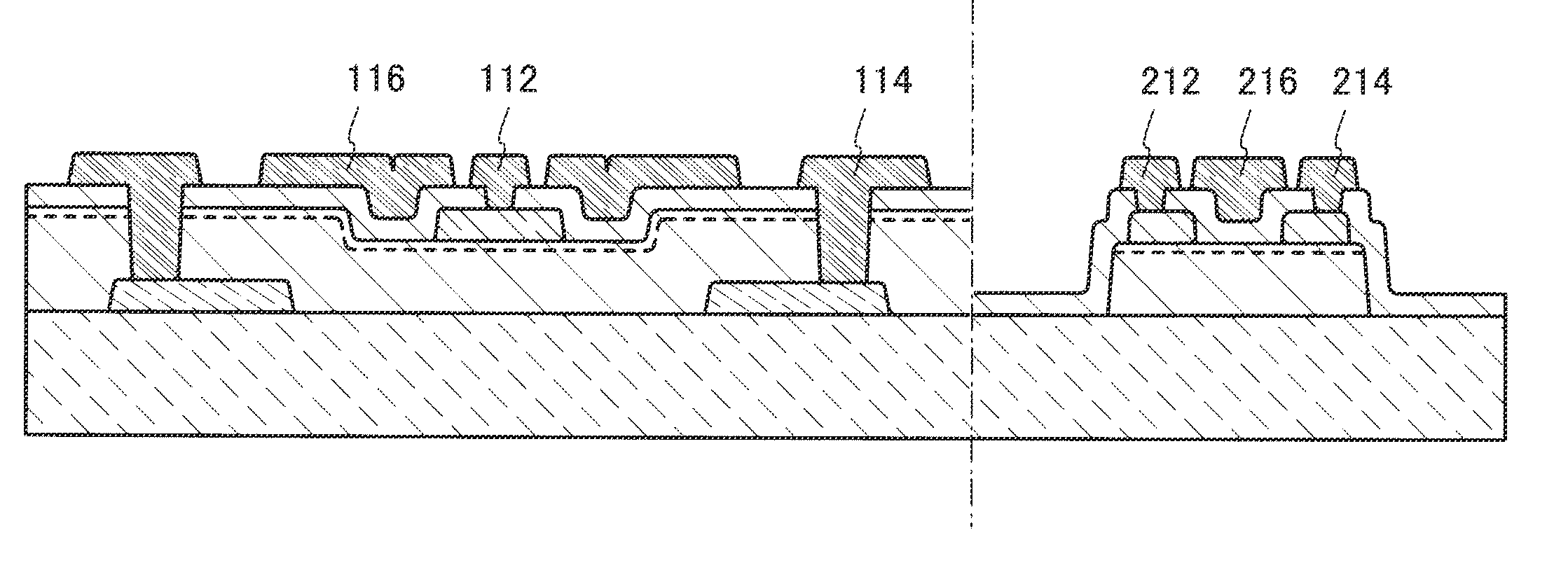
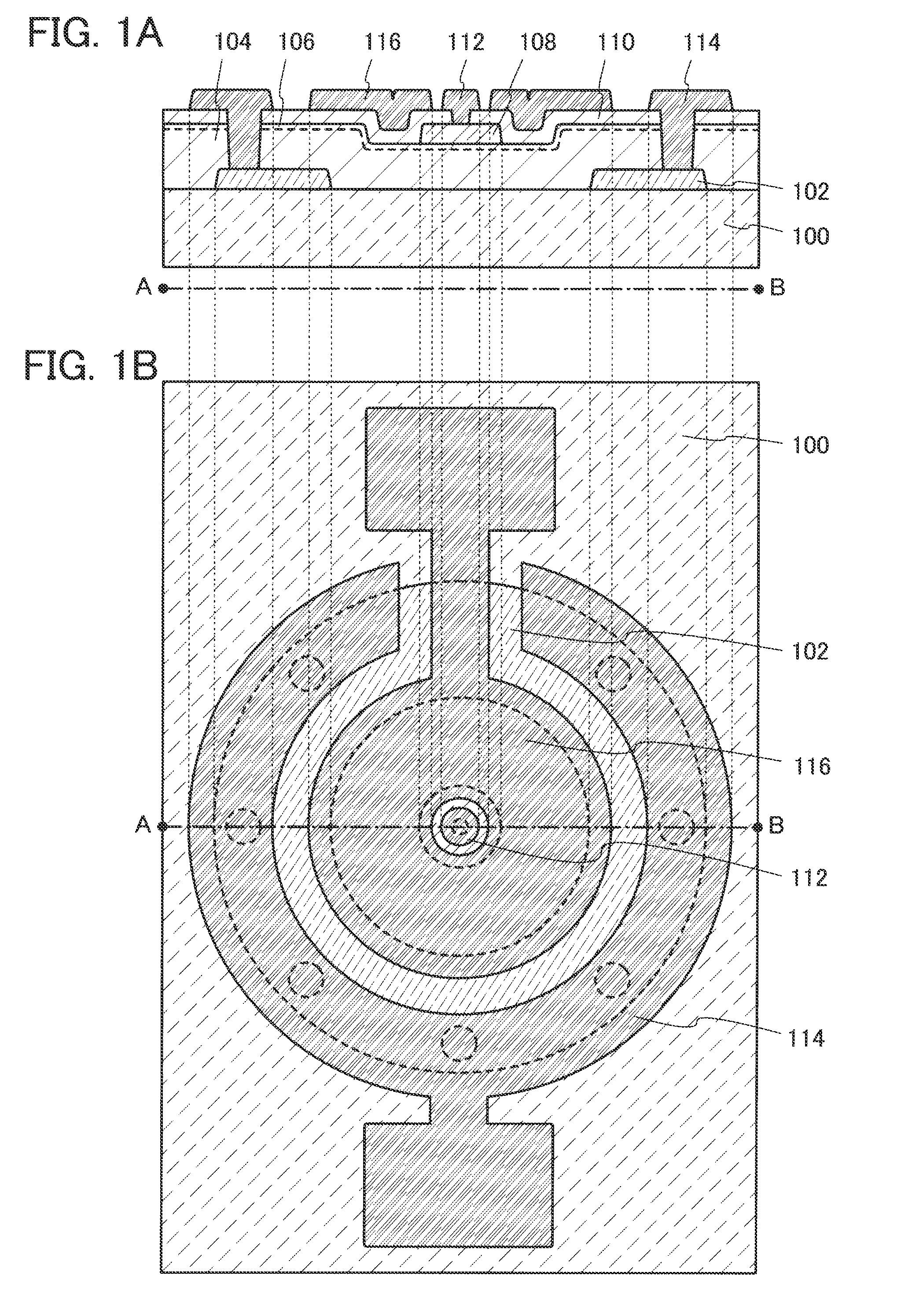
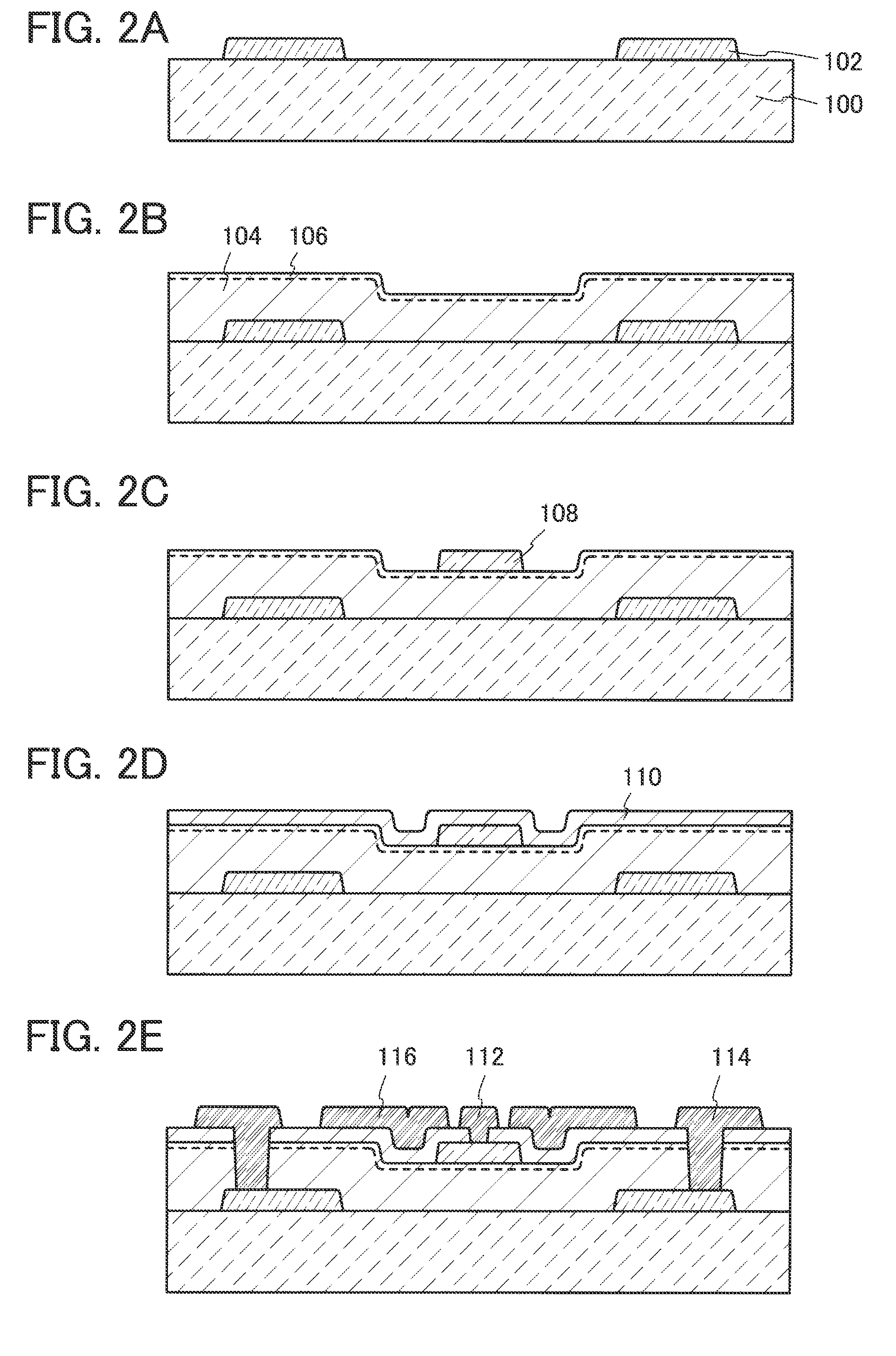
[0054]FIGS. 1A and 1B illustrate an example of a structure of a semiconductor device. FIG 1A is a cross-sectional view and FIG. 1B is a plan view. FIG 1A corresponds to a cross section along line A-B in FIG. 1B. Note that in the plan view, some components are omitted for ease of understanding.

[0055]The semiconductor device illustrated in FIGS. 1A and 1B includes the following: a substrate 100, a conductive layer 102 serving as one of a source electrode and a drain electrode, an oxide semiconductor layer 104, a crystal region 106 in the oxide semiconductor layer 104, a conductive layer 108 serving as the other of the source electrode and the drain electrode, an insulating layer 110 serving as a gate insulating layer, a conductive...

embodiment 2

[0109]In this embodiment, another example of a semiconductor device and a manufacturing method thereof will be described with reference to FIGS. 3A and 3B and FIGS. 4A to 4E. Note that there are many common points between the semiconductor device described in this embodiment and the semiconductor device according to the above embodiment. Therefore, the common points will be omitted, and different points will be mainly described.

[0110]FIGS. 3A and 3B illustrate another example of a structure of a semiconductor device. FIG. 3A is a cross-sectional view, and FIG. 3B is a plan view. FIG. 3A corresponds to a cross section along line C-D in FIG. 3B.

[0111]Components of the semiconductor device illustrated in FIGS. 3A and 3B are similar to those of the semiconductor device illustrated in FIGS. 1A and 1B. That is, the semiconductor device includes the following: a substrate 100, a conductive layer 102 serving as one of a source electrode and a drain electrode, an oxide semiconductor layer 12...

embodiment 3

[0121]In this embodiment, another example of a semiconductor device and a manufacturing method thereof will be described with reference to FIGS. 5A and 5B and FIGS. 6A to 6D. Note that there are many common points between the semiconductor device described in this embodiment and the semiconductor devices according to the above embodiments. Therefore, the common points will be omitted, and different points will be mainly described.

[0122]FIGS. 5A and 5B illustrate another example of a structure of a semiconductor device. FIG. 5A is a cross-sectional view and FIG. 5B is a plan view. FIG. 5A corresponds to a cross section along line E-F in FIG. 5B.

[0123]The semiconductor device illustrated in FIGS. 5A and 5B corresponds to a device in which the conductive layer 102 of the semiconductor device illustrated in any of the above embodiments is replaced with a conductive layer 109. That is, the semiconductor device illustrated in FIGS. 5A and 5B includes the following: a substrate 100; an oxi...


PUM


Abstract

The semiconductor device includes a first conductive layer over a substrate; an oxide semiconductor layer which covers the first conductive layer; a second conductive layer in a region which is not overlapped with the first conductive layer over the oxide semiconductor layer; an insulating layer which covers the oxide semiconductor layer and the second conductive layer; and a third conductive layer in a region including at least a region which is not overlapped with the first conductive layer or the second conductive layer over the insulating layer.

Description

BACKGROUND OF THE INVENTION[0001]1. Field of the Invention[0002]The technical field of the disclosed invention relates to a semiconductor device and a manufacturing method thereof.[0003]2. Description of the Related Art[0004]There are a wide variety of metal oxides and such metal oxides are used for various applications. Indium oxide is a well-known material and is used as a transparent electrode material which is necessary for liquid crystal displays and the like.[0005]Some metal oxides have semiconductor characteristics. The examples of such metal oxides having semiconductor characteristics are, for example, tungsten oxide, tin oxide, indium oxide, zinc oxide, and the like. A thin film transistor in which a channel formation region is formed using such metal oxides is already known (for example, see Patent Documents 1 to 4, Non-Patent Document 1, and the like).[0006]As metal oxides, not only single-component oxides but also multi-component oxides are known. For example, InGaO3(ZnO...

Claims


Application Information

Patent Timeline
IPC IPC(8): G05F1/10H01L29/26H01L21/20
CPCH01L21/0237H01L21/02554H01L29/66969H01L29/7869H01L21/02565H01L29/04H01L29/24H01L29/41733H01L29/42384
Inventor YAMAZAKI, SHUNPEITAKAHASHI, KEIITO, YOSHIAKI
Owner SEMICON ENERGY LAB CO LTD
Why Eureka
Try Eureka