

High voltage MOSFET diode reverse recovery by minimizing P-body charges
a technology of mosfet diodes and reverse recovery, which is applied in the direction of diodes, semiconductor devices, electrical apparatus, etc., can solve the problems of large turn off time and loss, igbt devices implemented for power supply and motor control applications often suffer from limitations of high qrr and power loss, and adversely affect production costs
- Summary
- Abstract
- Description
- Claims
- Application Information
AI Technical Summary
Benefits of technology
Problems solved by technology
Method used
Image

Examples
Embodiment Construction
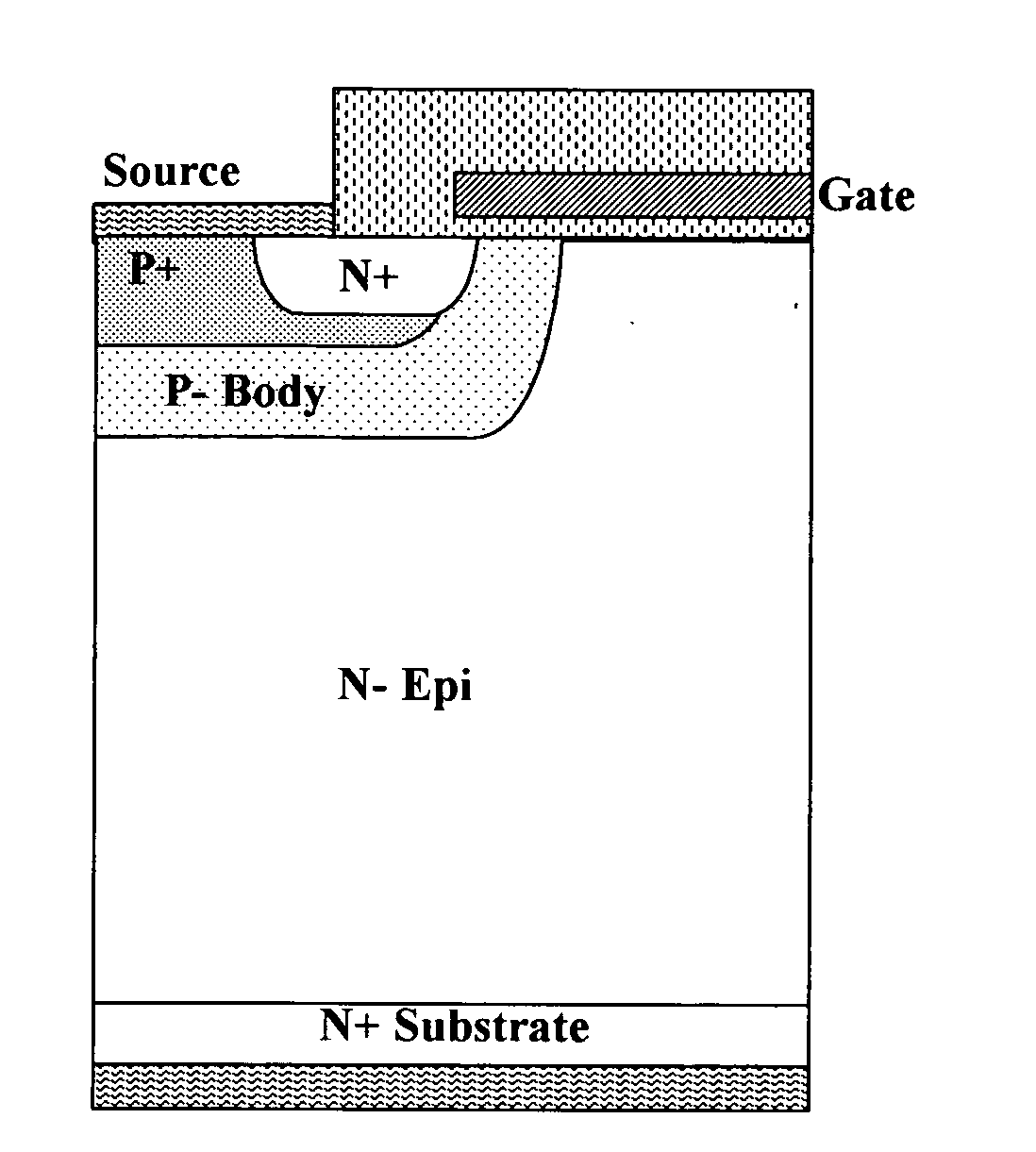
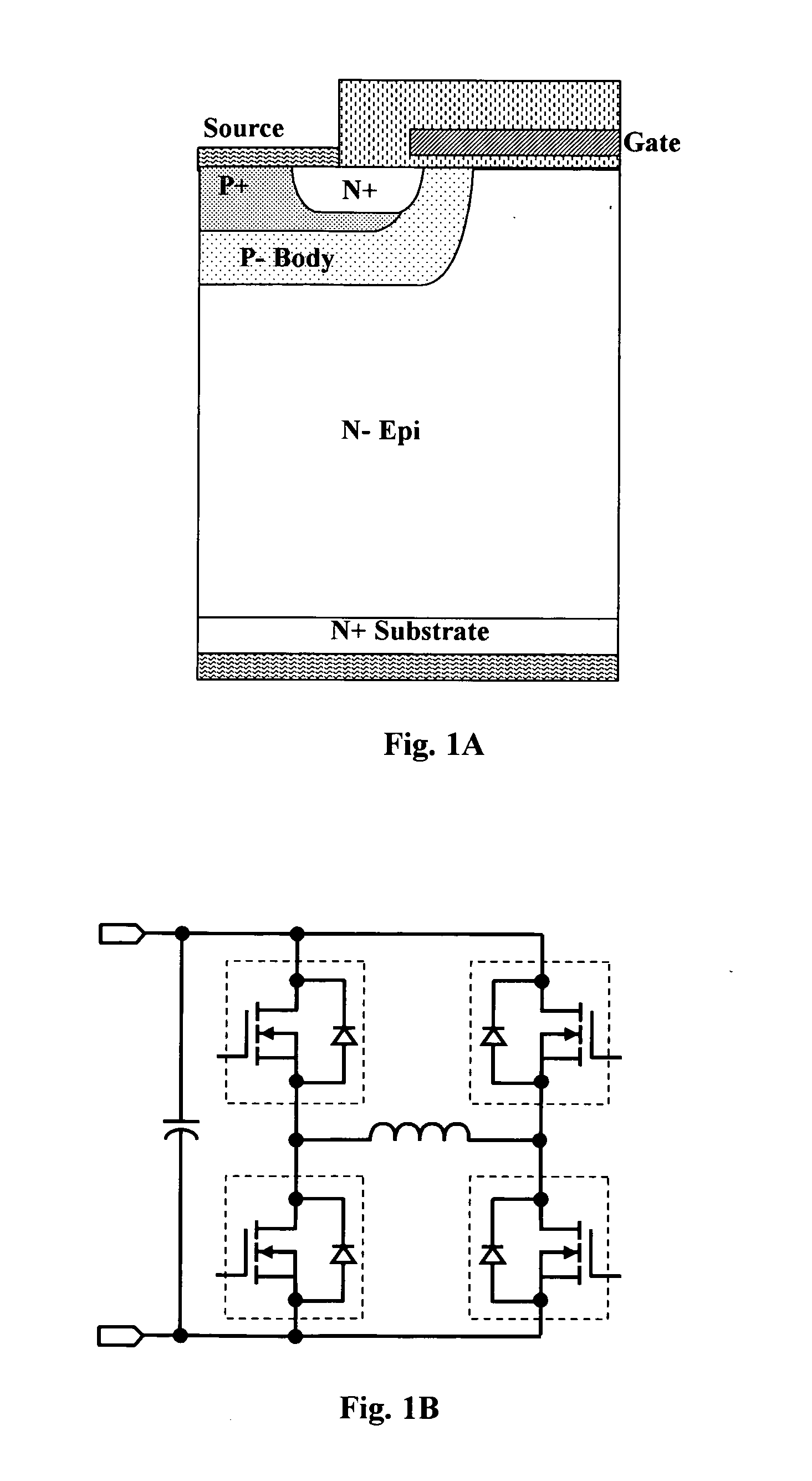
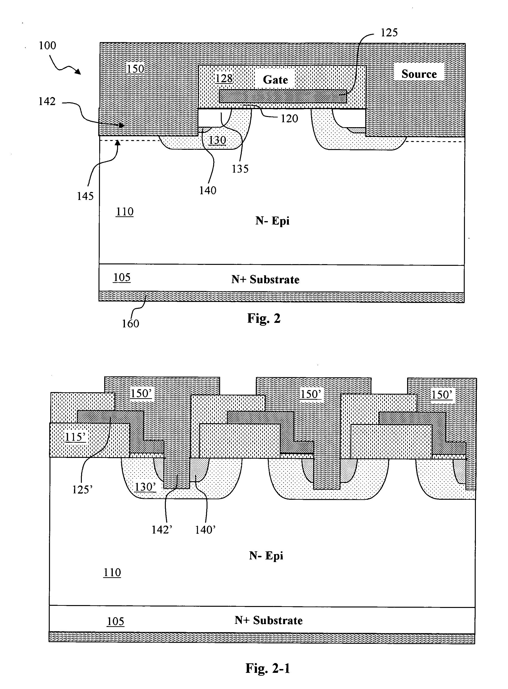
[0028]Referring to FIG. 2 for a cross sectional view of active cell 100 of a high voltage MOSFET (HV MOSFET) semiconductor power device of this invention. The HV MOSFET device is supported on an N+ silicon substrate 105 with an epitaxial layer 110 formed on top of the N+ substrate 105. A planar gate 125 is formed on top of a gate oxide layer 120. A P-body region 130 is formed in the epitaxial layer below the gate oxide layer 120 encompassing an N+ source region 135. The MOSFET device 100 further includes a P+ doped region 140 within the P-body region 130. A source metal 150 covering the top surface with direct contact to the source region 135 and the P-body region 130. A drain metal 160 to function as a drain electrode is formed on the back side of the semiconductor substrate 105 thus forming an active cell of vertical MOSFET power device. The drawing is not to scale, as the substrate 105 is typically several times thicker than the epitaxial layer 110. A contact trench 142 is formed...
PUM
 Abstract
Description
Claims
Application Information