
Method and apparatus for controlled thermal processing

a controlled thermal processing and method technology, applied in microwave heating, heat measurement, optical radiation measurement, etc., can solve the problems of destroying silicon crystal structures, knocking out silicon atoms, and demanding low thermal budgets

Active Publication Date: 2011-03-31
APPLIED MATERIALS INC
View PDF6 Cites 14 Cited by
  • Summary
  • Abstract
  • Description
  • Claims
  • Application Information

AI Technical Summary

Benefits of technology

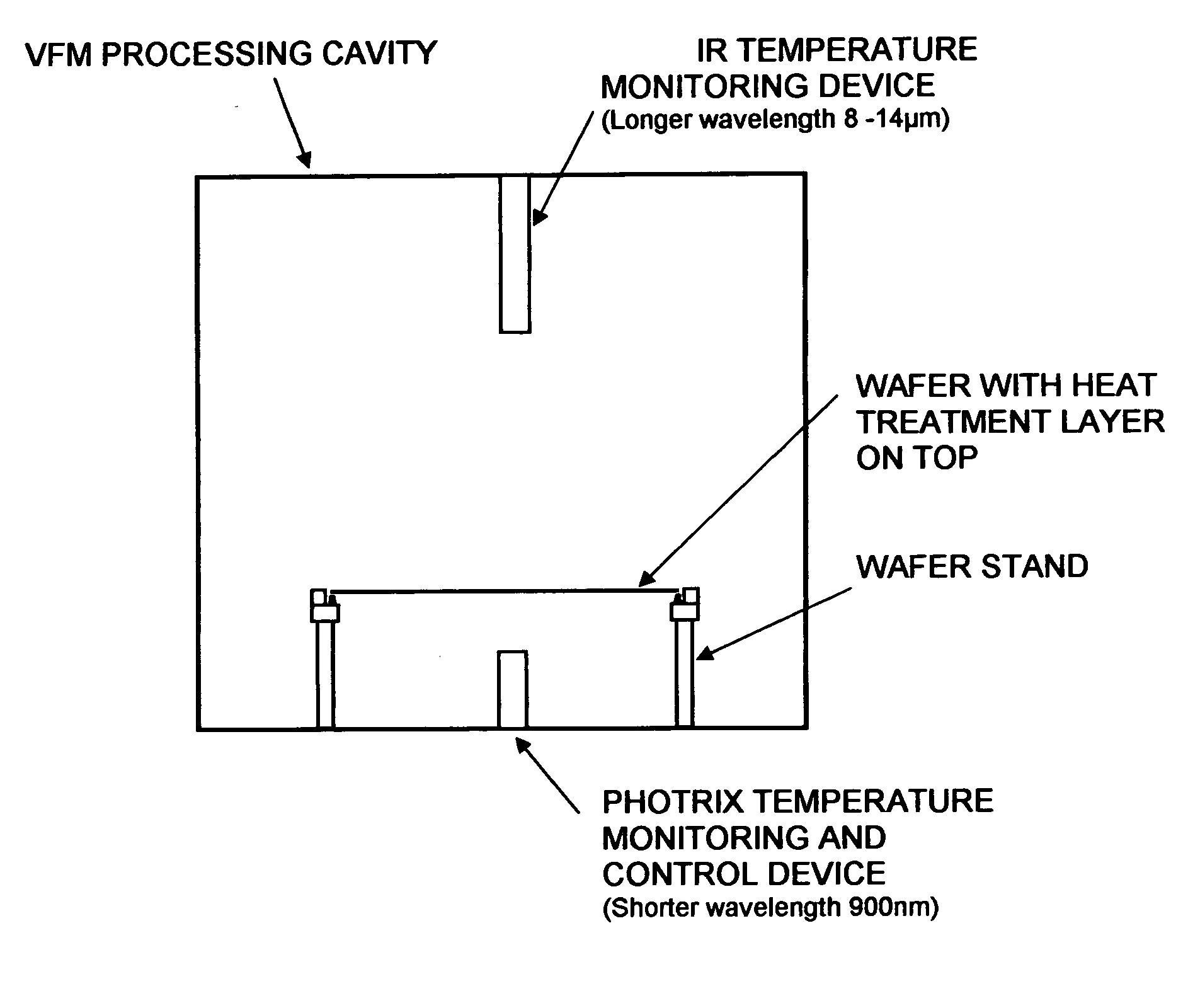
[0022]According to one aspect of the invention, an apparatus for processing semiconductors comprises: a thermal processing chamber including a heating source; a first noncontacting thermal measurement device positioned to measure temperature on a first area of the semiconductor; and a second noncontacting thermal measurement device positioned to measure temperature on a second area of the semiconductor, the first device being relatively more sensitive to changes in surface emissivity than the second device.

Problems solved by technology

During the ion implantation process the heavy ions easily knock out silicon atoms and silicon crystal structure is damaged.
These shallow junctions demand low thermal budgets, requiring processing at a high ramp rate with minimal peak temperature overshoot.
The steep thermal profiles give the best junction characteristics by limiting dopant diffusion but challenges the ability to deliver consistent process uniformity and repeatability.
The primary challenge is production worthiness, measured by within-wafer uniformity and wafer-to-wafer repeatability, to get product yield from the wafer edge especially as device geometries shrink, where an even shallower junction must be ensured.
Metal silicides have been widely applied to IC fabrication because of their high melting points and low resistance.
However, the nickel-silicon system has various phases (i.e., the phase diagram is more complex than the Co—Si system) and typically undergoes phase transformation during the heating cycle.
Similarly, the identification of NiSi will not be easy since the Ni2Si and Ni3Si2 phases are also orthogonal.
The oxide growth does not create significant stresses in the material that can lead to serious problems including circuit failure.
However, fast oxidation leaves more dangling bonds at the silicon interface, which allows current to leak along the interface.
Wet oxidation also yields a lower density oxide with lower dielectric strength.
The high temperature spikes may also lead to warping of the wafer and uncontrollable strain in the device structure.

Method used


Image

  • Method and apparatus for controlled thermal processing
  • Method and apparatus for controlled thermal processing
  • Method and apparatus for controlled thermal processing

Examples


example

Wafer Oxidation

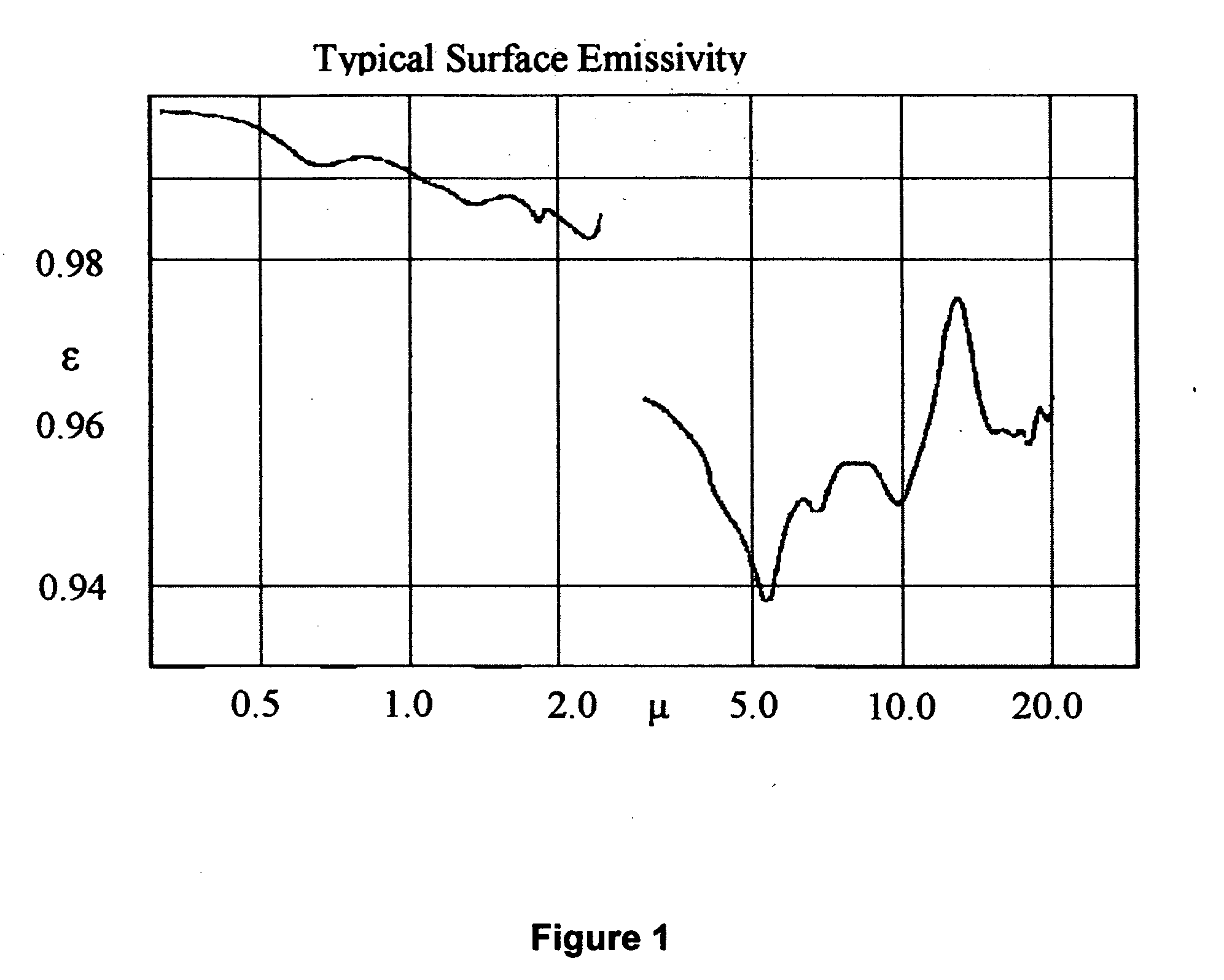
[0062]As noted earlier, the oxidation of silicon to form SiO2 as an insulating dielectric layer in semiconductor device fabrication is another critical process in modern semiconductor manufacturing. A bare silicon surface has emissivity of 0.6-0.8 depending on the finish on the surface. During the oxidation process, as silicon dioxide grows on the surface, the emissivity will typically increase to a value characteristic of SiO2 (∈=0.95) which, as in the two preceding examples, lends itself to the inventive method in which apparent temperature as monitored by the IR temperature device could be used determine the progress of the oxidation process.

[0063]Based on the foregoing examples, the skilled artisan will appreciate that the inventive method can be used to improve process control in many processes of interest to the semiconductor manufacturer. The inventive apparatus can be constructed using readily available components, and the inventive method can be adapted to a ...


PUM

PropertyMeasurementUnit
temperaturesaaaaaaaaaa
soak temperatureaaaaaaaaaa

Abstract

A materials processing system comprises a thermal processing chamber including a heating source, a first noncontacting thermal measurement device positioned to measure temperature on a first area of the material being processed, and, a second noncontacting thermal measurement device positioned to measure temperature on a second area of the material being processed, the first device being relatively more sensitive to changes in surface emissivity than the second device. By comparing the outputs of the two devices, emissivity changes can be detected and used as a proxy for some physical change in the workpiece and thereby determine when the desired process has been completed. The system may be used to develop a process recipe, or it may be part of a system for real-time process control based on emissivity changes. Applicable processes include heating, annealing, dopant activation, silicide formation, carburization, nitridation, sintering, oxidation, vapor deposition, metallization, and plating.

Description

CROSS REFERENCE TO RELATED APPLICATION[0001]This application claims the benefit of U.S. Provisional Application Ser. No. 61 / 277,542, filed on Sep. 25, 2009 by the present inventors, the entire disclosure of which is incorporated herein by reference.BACKGROUND OF THE INVENTION[0002]1. Field of the Invention[0003]The invention pertains to the field of heat treating materials using microwave energy. More particularly the invention pertains to apparatus and methods for heating silicon wafers while monitoring the wafer temperature.[0004]2. Description of Related Art[0005]Furnace annealing is a process used in semiconductor device fabrication wherein a batch of semiconductor wafers is heated in order to affect their electrical properties. Wafers can be heated in order to activate dopants, change film-to-film or film-to-wafer substrate interfaces, change states of grown films, densify deposited films, repair damage from implantation, diffuse dopants or drive dopants from one film into anot...

Claims


Application Information

Patent Timeline
Patent Type & Authority Applications(United States)
IPC IPC(8): H01L21/66H05B3/02H05B6/64A21B1/00
CPCG01J5/0007H05B6/806H01L21/67248G01J2005/0051G01J5/802
Inventor AHMAD, IFTIKHARHICKS, KEITH R.
Owner APPLIED MATERIALS INC
Learn More