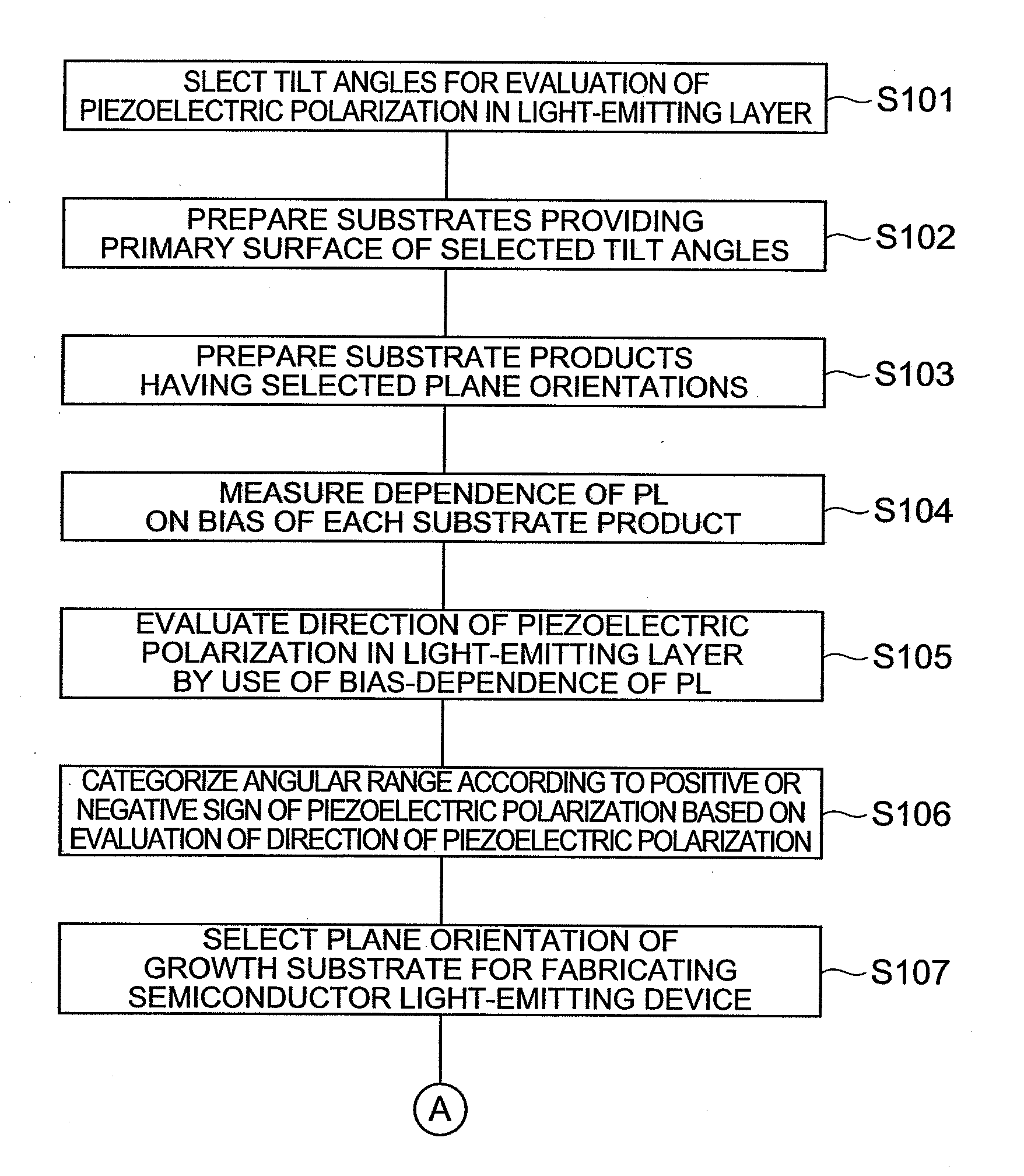
Method of making semiconductor light- emitting device
- Summary
- Abstract
- Description
- Claims
- Application Information
AI Technical Summary
Benefits of technology
Problems solved by technology
Method used
Image

Examples
example 1
[0095]Devices 1 to 9 including light-emitting diodes (LEDs) are prepared. FIG. 7 illustrates the LED structure of Devices 1 to 9. Device 2 and
[0096]Device 6 are formed on a polar surface and a non-polar surface, respectively. GaN substrates 71 having plane orientations corresponding to Devices 1 to 9 are prepared for the LED structure shown in FIG. 7. The primary surface 71a of each GaN substrate 71 had a plane orientation and an off-angle listed in FIG. 8. The off-angle α is defined by the reference plane Sc perpendicular to the reference axis Cx extending along the c-axis, and the primary surface. The GaN substrate 71 is loaded into a reactor, and ammonia (NH3) and hydrogen (H2) are supplied to the reactor. The GaN substrate 71 is kept at temperature of 1050 degrees Celsius for 10 minutes. After this pretreatment (thermal cleaning), source gases are fed to fabricate an epitaxial laminate structure by metalorganic vapor phase epitaxy, as described below.
[0097]An n-type GaN layer 72...
PUM
 Abstract
Description
Claims
Application Information