Highly Power-efficient and Broadband Quantum Cascade Lasers

a quantum cascade laser, high-power-efficient technology, applied in lasers, lasers, semiconductor lasers, etc., can solve the problems of uneven interface between adjacent semiconductor layers, large increase in the number of quantum cascade lasers, and poor temperature performance, and achieve wide gain spectrum, good temperature performance, and large gain spectrum width

Inactive Publication Date: 2011-04-07
THE JOHN HOPKINS UNIV SCHOOL OF MEDICINE +1
View PDF1 Cites 11 Cited by
  • Summary
  • Abstract
  • Description
  • Claims
  • Application Information

AI Technical Summary

Benefits of technology

[0009]In a further aspect, the present invention provides QC laser designs with two lower injector states, rather than one, strongly coupled with the upper laser state at the operating electric fields. Optical transitions from all three states to the lower laser state contribute to a broad gain spectrum; hence we term such designs as “continuum-to-bound” designs. Exemplary QC laser designs may operate at 7-9 μm with two lower injector states strongly coupled with the upper laser state at the operating electric fields. Optical transitions from these three coupled states contribute to a large gain spectrum width (−250 cm−1 full width at half maximum), which enables external cavity tuning of the lasers over 200 cm−1. The exemplary lasers show comparable performance to a conventional narrow band design at a similar wavelength with a peak modal gain coefficient of ˜10 kA / cm, a slope efficiency ˜1 W / A and good temperature performance (T0=170 K) in pulsed mode operation at 295 K.

Problems solved by technology

However, advances were largely incremental, and especially the basic quantum design had remained unchanged for many years, with the WPE yet to reach above 35%.
With practical growth techniques, interfaces between adjacent semiconductor layers are not perfectly smooth, but in fact are rather rough on the scale of atomic layer steps of a few Å, which is significant compared to the typical semiconductor layer thicknesses of ˜10-50 Å in QC lasers.
This effect has been greatly underestimated until recently, so that conventional designs failed to incorporate an adequate mechanism to reduce its negative influence.
Apart from roughness-induced inefficiencies, broadly tunable QC lasers are ideal candidates for multi-analyte mid-infrared spectroscopy applications; however, the maximum tuning range is usually limited by the inherently narrow linewidth of intersubband transitions.

Method used


Image

  • Highly Power-efficient and Broadband Quantum Cascade Lasers
  • Highly Power-efficient and Broadband Quantum Cascade Lasers
  • Highly Power-efficient and Broadband Quantum Cascade Lasers

Examples


example 1

[0042]Exemplary QC laser structures (and electroluminescent structures) according to the design of FIG. 2 were grown by metal organic chemical vapor deposition (MOCVD) on InP substrate using strain-balanced In0.660Ga0.340As / Al0.690In0.310As materials and consisted of a low-loss InP-based waveguide cladding on top of 43 repeats of the injector / active regions sequence. Each injector region had a sheet doping density of 1×1011 cm−2. Ridge-waveguide lasers were fabricated with ridge widths varying from 13.5-21.5 μm using conventional III-V semiconductor processing techniques. The ridges were wet-etched to ˜8 μm deep, a ˜0.3 μm SiOx insulation layer was deposited with PECVD, thin 30 / 300 nm Ti / Au top metal contacts were deposited through electron-beam evaporation, the substrate was then thinned down to ˜200 μm, and a 20 / 200 nm Ge / Au bottom metal contact was deposited. Exemplary devices with cavity lengths varying from 0.5-4.0 mm and as-cleaved facets were mounted epitaxial-side up to copp...

example 2

[0046]Exemplary QC laser structures according to the design of FIG. 7 were grown by metal organic chemical vapour deposition (MOCVD) on InP substrate using strain-balanced In0.652Ga0.348As / Al0.690In0.310As and consisted of a low-loss InP-based waveguide surrounding 41 repeats of the injector—active region sequence. The injector had a sheet doping density of 1×1011cm−2. Electroluminescence (EL) structures were fabricated as deep-etched, 200 μm diameter mesas with Ti / Au (250 / 2500 Å) top and Ge / Au (250 / 2500 Å) bottom contacts. The mesas were mounted to a copper heat sink. The lasers were fabricated as deep-etched ridge waveguide lasers with ridge width of around 10 μm and SiO2 (3300 Å) for side-wall electrical insulation. The devices were thinned to ˜200 μm and top Ti / Au (230 / 2500 Å) and bottom Ge / Au (230 / 2500 Å) contacts were deposited. The ridges were cleaved to various lengths and mounted epitaxial side up to copper heat sinks.

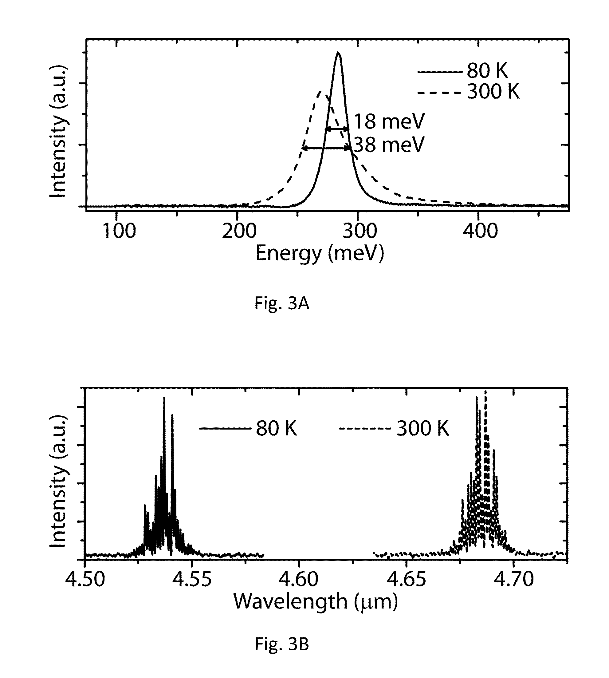
[0047]Electroluminescence spectra were collected for var...

examples

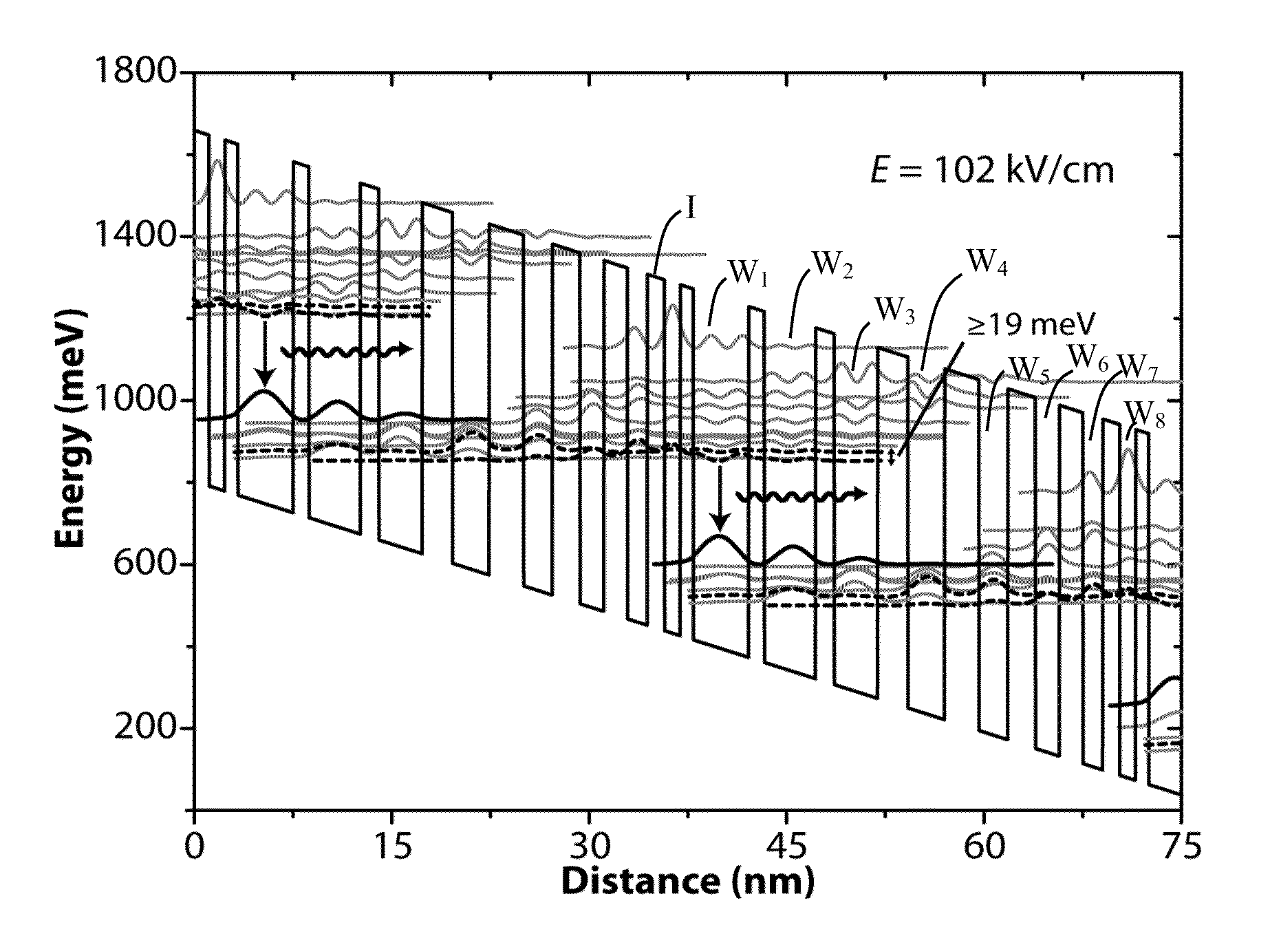
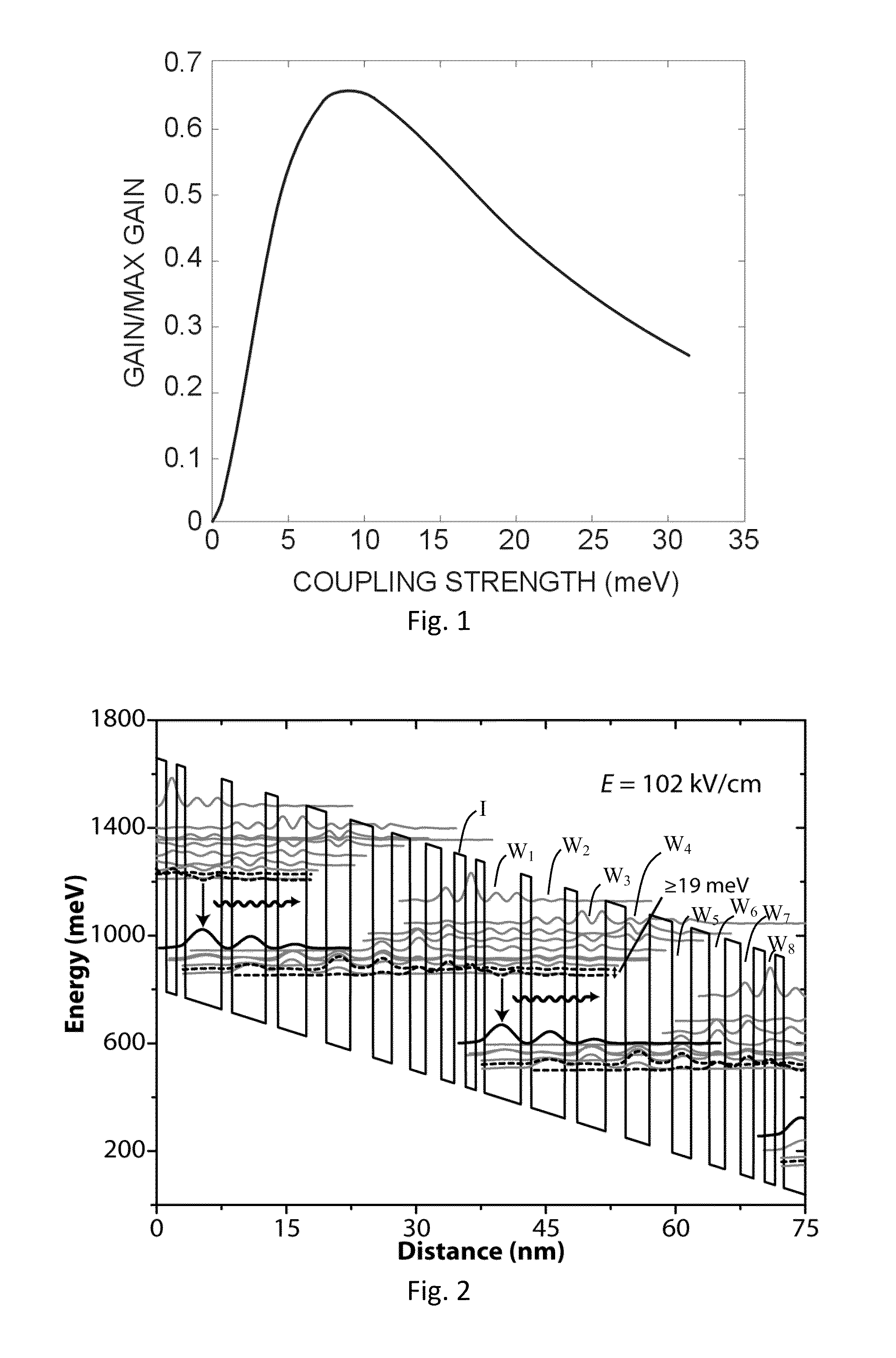
[0052]Exemplary prototype devices based on designs A and B (with the continuum-to-bound active regions) were grown by solid source molecular beam epitaxy (MBE) with InGaAs / InAlAs quantum wells lattice-matched to an InP low-doped substrate (doped n˜1−2×1017 cm−3). The active core included 40 periods of injector and active regions. A 0.6 μm InGaAs (doped n˜5×1016 cm−3) layer was grown below the active region for mode confinement; a 0.3 μm InGaAs (doped n˜5×1016 cm−3) top mode confinement layer and a 2.8 μm AlInAs (doped n˜1×1017 cm−3) top cladding layer were grown above the active core, followed by a 0.6 μm InGaAs plasmon layer (doped n˜1×1019 cm−3) and a final 300 Å thick layer of InGaAs (doped n˜2×1019 cm−3) as the contact layer. The wafer was processed into 200 μm diameter circular mesas as well as deep-etched ridge lasers with different ridge widths (from 11 to 20 μm).

[0053]Electroluminescence from a semi-circular cleaved mesa based on design A (˜23 meV splitting) was measured at ...


PUM


Abstract

The present invention relates generally to highly power-efficient quantum cascade sources, such as highly power-efficient quantum cascade lasers having ultra-strong coupling between injector and active regions which may be configured to provide broadband quantum cascade lasers.

Description

RELATED APPLICATIONS[0001]This application claims the benefit of priority of U.S. Provisional Application No. 61 / 185,182, filed on Jun. 8, 2009, the entire contents of which application are incorporated herein by reference.GOVERNMENT LICENSE RIGHTS[0002]This invention was made with government support under Grant No. EECO540832 awarded by the National Science Foundation and Grant No. FA8650-07-1-7708 awarded by the United States Air Force (USAF / AFMC). The government has certain rights in this invention.FIELD OF THE INVENTION[0003]The present invention relates generally to highly power-efficient quantum cascade sources, and more particularly, but not exclusively, to highly power-efficient quantum cascade lasers having ultra-strong coupling between injector and active regions which may be configured to provide broadband quantum cascade lasers.BACKGROUND[0004]Quantum Cascade (QC) lasers are ideal mid-infrared semiconductor light sources for molecular detection in applications such as en...

Claims


Application Information

Patent Timeline
Patent Type & Authority Applications(United States)
IPC IPC(8): H01S5/34
CPCB82Y20/00H01S5/3407H01S5/3402H01S5/0014
Inventor LIU, QIANGYAO, YUHOFFMAN, ANTHONY J.ESCARRA, MATTHEWFRANZ, KALE J.KHURGIN, JACOBDIKMELIK, YAMACCHARLES, WILLIAM O.CHEN, JIANXINGMACHL, CLAIRE F.
Owner THE JOHN HOPKINS UNIV SCHOOL OF MEDICINE
Why Eureka
Try Eureka