Photomask blank and method for manufacturing the same
a technology of photomask and photomask, which is applied in the field of photomask blank, photomask and photomask manufacturing method, can solve the problems of generating haze on the photomask due to washing with sulfuric acid, unusable portion irradiation, and unsuitable portion, and achieves high chemical resistance to ozone, not easily changed, and not easily decreased film thickness
- Summary
- Abstract
- Description
- Claims
- Application Information
AI Technical Summary
Benefits of technology
Problems solved by technology
Method used
Image
Examples
example 1
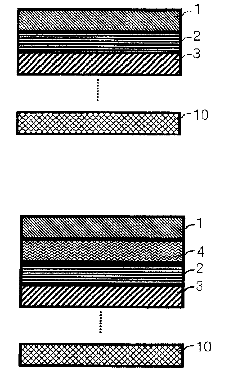
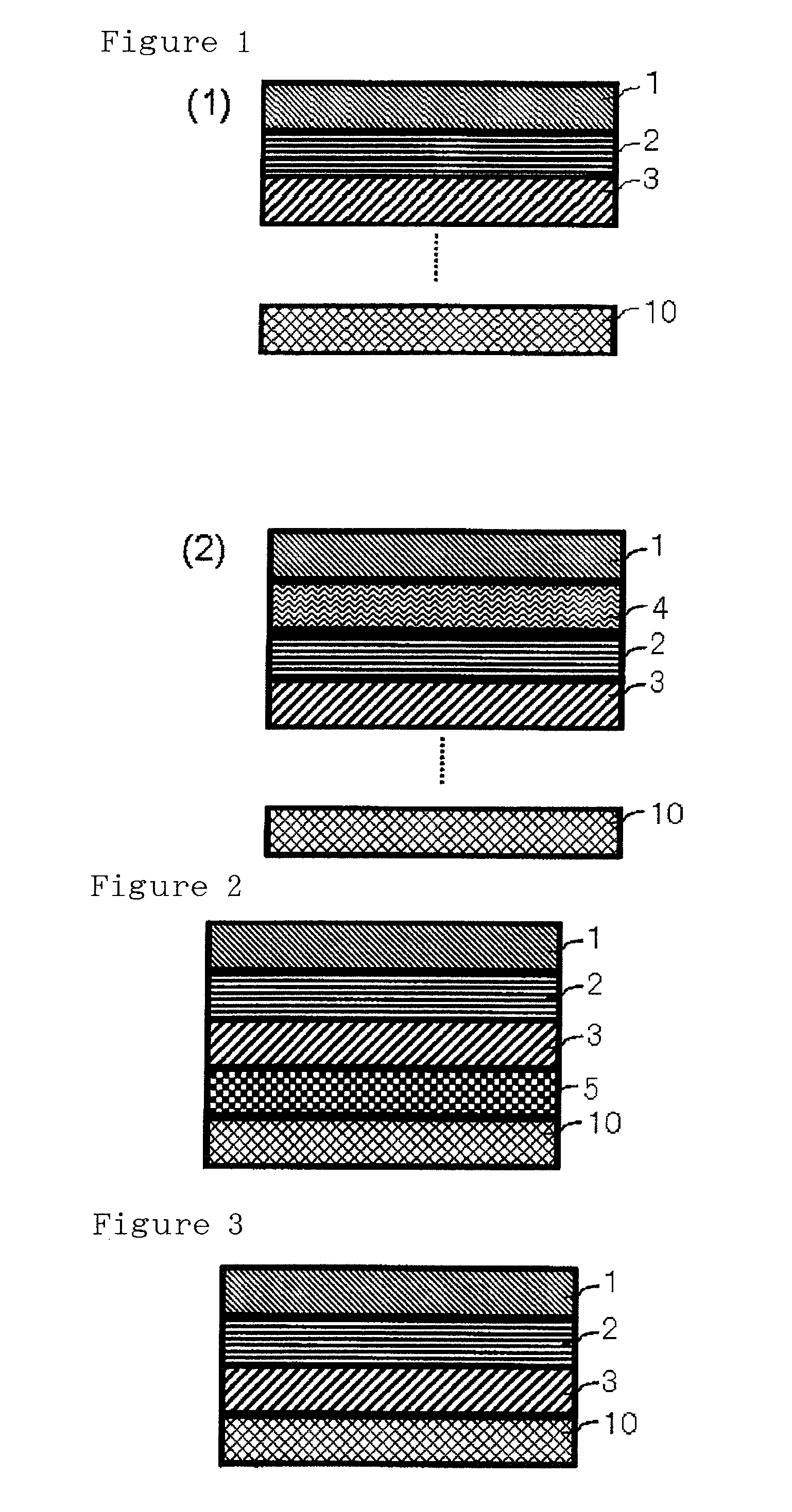
[0106]In this working example, a halftone phase shift mask blank, in which a phase shifter film 5 and a light-shielding film consisting of 3 layers are provided on a light transmissive substrate 10, was produced (see FIG. 2).
[0107]Firstly, on the light transmissive substrate 10 made of quartz glass having a size of 6-inch square and a thickness of 0.25 inch, a halftone phase shifter film 5 for ArF excimer laser (wavelength: 193 nm) constituted by a single layer comprising Mo, Si and N as the main components was formed (thickness: 69 nm) using a single-wafer sputtering apparatus.
[0108]As shown in Table 1, sputtering (DC sputtering) conditions are as follows:
Sputtering target: a mixed target of Mo and Si (Mo:Si=8:92 mol %)
Sputtering gas: a mixed gas atmosphere of Ar gas, N2 gas and He gas (Ar: 9 sccm, N2: 81 sccm, He: 76 sccm)
Gas pressure during discharge: 0.3 Pa
Applied power: 2.8 kW
[0109]When the ArF excimer laser light (wavelength: 193 nm) was applied, the transmittance of the obtai...
example 2
[0125]In this working example, a binary mask blank, in which a light-shielding film consisting of 3 layers is provided on a light transmissive substrate 10, was produced (see FIG. 3).
[0126]That is, reactive sputtering was carried out under the same conditions as those in Example 1 except that the conditions of sputtering were set as shown in Table 1.
[0127]Thus, a photomask blank as shown in FIG. 3, in which the back-surface antireflection layer 3, the light-shielding layer 2 and the front-surface layer 1 are laminated in this order on the light transmissive substrate 10 made of quartz glass, was obtained. The optical density (O.D.) of the light-shielding film consisting of the back-surface antireflection layer 3, the light-shielding layer 2 and the front-surface layer 1 with respect to light having a wavelength of 193.4 nm was 3.
[0128]Next, in the same manner as that in Example 1, the compositions of the front-surface layer 1, the light-shielding layer 2 and the back-surface antiref...
PUM
| Property | Measurement | Unit |
|---|---|---|
| thickness | aaaaa | aaaaa |
| grain size | aaaaa | aaaaa |
| wavelength | aaaaa | aaaaa |
Abstract
Description
Claims
Application Information
 - R&D
- Intellectual Property
- Life Sciences
- Materials
- Tech Scout
- Unparalleled Data Quality
- Higher Quality Content
- 60% Fewer Hallucinations
Browse by: Latest US Patents, China's latest patents, Technical Efficacy Thesaurus, Application Domain, Technology Topic, Popular Technical Reports.
© 2025 PatSnap. All rights reserved.Legal|Privacy policy|Modern Slavery Act Transparency Statement|Sitemap|About US| Contact US: help@patsnap.com


