Electrode and method for manufacturing the same
a technology of electric devices and electrodes, applied in the manufacture of electrode systems, electric discharge tubes/lamps, instruments, etc., can solve the problems of increasing capital investment, provoking a sharp rise in material costs, and copper cannot be sintered in air, so as to reduce the cost of production
- Summary
- Abstract
- Description
- Claims
- Application Information
AI Technical Summary
Benefits of technology
Problems solved by technology
Method used
Image
Examples
example 1
1. Preparation of Organic Components
[0104]Texanol (2,2,4-trimethyl-1,3-pentanediol monoisobutyrate) as the solvent and acrylic polymer binder having a molecular weight of 6,000 to 7,000 as the organic binder were mixed, and the mixture was heated to 100° C. while stirring. The mixture was heated and stirred until all of the organic binder had dissolved. The resulting solution was cooled to 75° C. EDAB (ethyl 4-dimethyl aminobenzoate), DETX (diethylthioxanthone), and Irgacure 907 by Chiba Specialty Chemicals were added as photo polymerization initiator, and TAOBN (1,4,4-trimethyl-2,3-diazabicyclo[3.2.2]-non-2-ene-N,N-dixoide) was added as a stabilizer. The mixture was stirred at 75° C. until all the solids had dissolved. The solution was filtered through a 40 micron filter and cooled.
2. Preparation of Paste
2-1: Preparation of Paste 1 (Cu)
[0105]A photopolymerization monomer consisting of 2.62 wt % TMPEOTA (trimethylolpropane ethoxytriacrylate), 2.62 wt % Laromer® LR8967 (polyethyl acr...
examples 2-5
, Comparative Examples 7-8
[0130]Pattern forming was attempted using Paste 2 (B), Paste 3 (Cu), and Paste 4 (Ni) shown in Table 1.
TABLE 4ComparativeComparativeEx. 2Ex. 3Ex. 7Ex. 8Ex. 4Ex. 5Top LayerPaste 2 (B)Paste 2 (B)NoneNonePaste 2 (B)Paste 2 (B)Bottom LayerPaste 3 (Cu)Paste 4 (Ni)Paste 3 (Cu)Paste 4 (Ni)Paste 3 (Cu)Paste 4 (Ni)Thickness of dried film11.7511.4 5.259.35(um)Surface resistance Ohm 0.1954.5859115004.00E+07——Volume resistivity Ohm · cm1.28E−056.98E−04N / MN / M2.21E−055.31E−04Photo patterningOKOK——OKOK
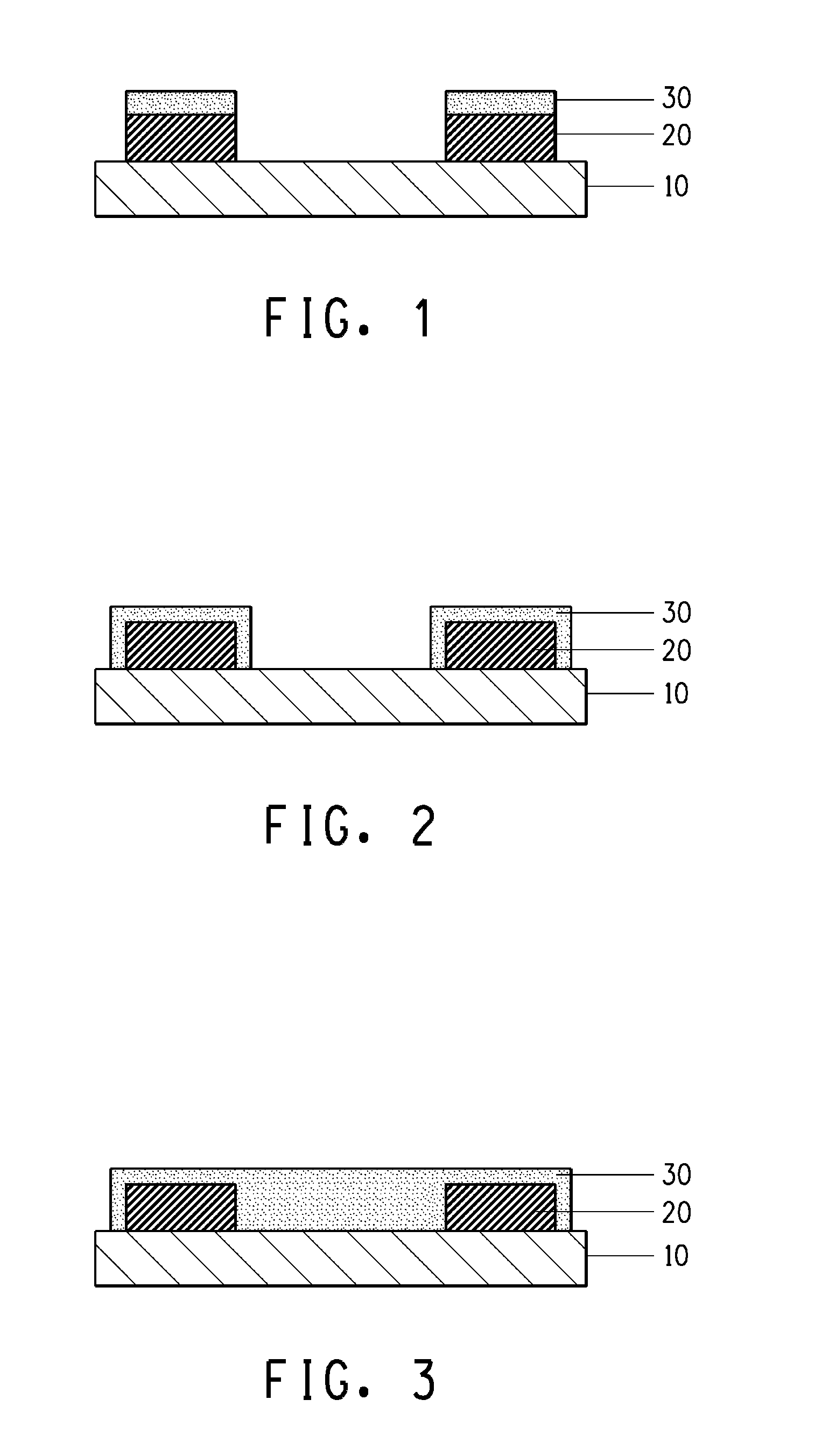
[0131]For Examples 2 and 3 in Table 4, the bottom layer was configured by coating and drying a paste containing copper or nickel conductive powder, respectively, and after a paste containing boron was coated as the top layer, the bilayer dried films were exposed and developed. In this case the cross-sectional structure of the formed pattern is the one illustrated in FIG. 1. In Example 2 the surface resistance was 0.195Ω and the volume resistivity was 1.28×10⁻⁵Ω·cm, and ...
examples 6-8
, Comparative Examples 9-11
[0133]Pattern forming was attempted using Paste 5 (Cu+Sn), Paste 6 (Bi+Sn), Paste 7 (Cu+solder), and Paste 8 (B) shown in Table 5.
TABLE 5Paste 5Paste 6Paste 7Paste 8(Cu + Sn)(Bi + Sn)(Cu + Solder)(B)Medium (binder, initiator, solvent)18.0013.1713.1742.76Antifoamer (silicone oil)0.38Dispersant (Soya lecithin)0.580.610.61Malonic acid (viscosity stabilizer)1.83Solvent (Texanol)0.450.480.485.24Monomer28.76(TMPEOTA:Laromer ® LR8967:Sartomer ® SR399 = 1:1:3)Glass frit (Nippon Yamamura Glass)2.903.073.070.26Boron (H. C. Starck, Grade I)20.77Braze Tec CTF600, Cu 76, Sn 15, Ni 4,78.07P 5 Alloy in a form of thermoplastic paste, Tm 590-600 C. Mitsui Kinzoku, Sn 42% / Bi 58% 82.68alloy, 5 um powderMitsui Kinzoku, SAC305,41.34Sn 96.5% / Ag 3% Cu 0.5%, Pb-freesolder alloy, 5 um powderCopper (DOWA electronics, 41.34D50 = 1.0 m)Total100.00100.00100.00100.00
[0134]Resistance was measured in the fired films prepared by configuring a conductive layer using pastes containing the v...
PUM
 Abstract
Description
Claims
Application Information


