

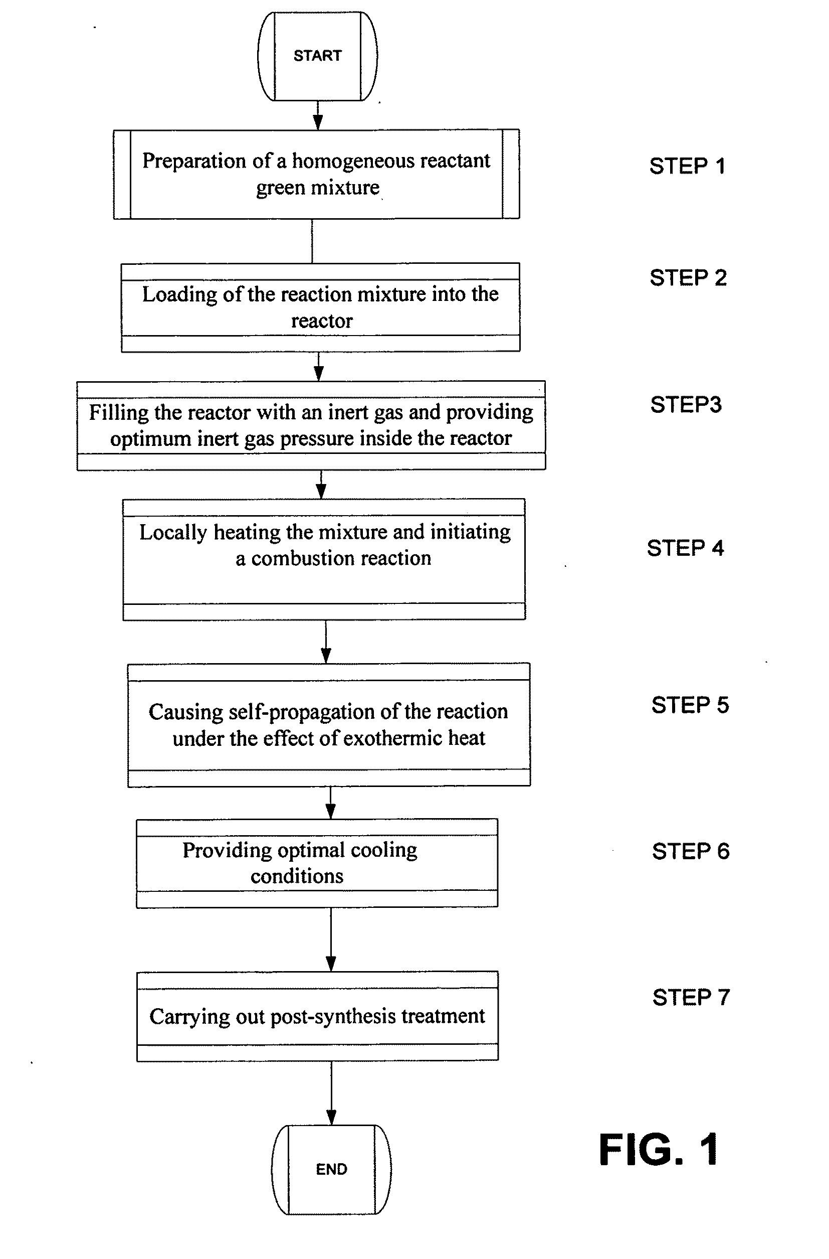
Method of manufacturing high-surface-area silicon
a manufacturing method and silicon technology, applied in the field of materials synthesis, can solve the problems of abnormally difficult and expensive process of silicon purification, high cost, and energy consumption of conventional methods, and achieve the effects of high surface area, high purity, and high efficiency and flexibility
- Summary
- Abstract
- Description
- Claims
- Application Information
AI Technical Summary
Benefits of technology
Problems solved by technology
Method used
Image

Examples
Embodiment Construction
[0033]Prior to describing the invention, it is advantageous to define terminology used herein, as follows.
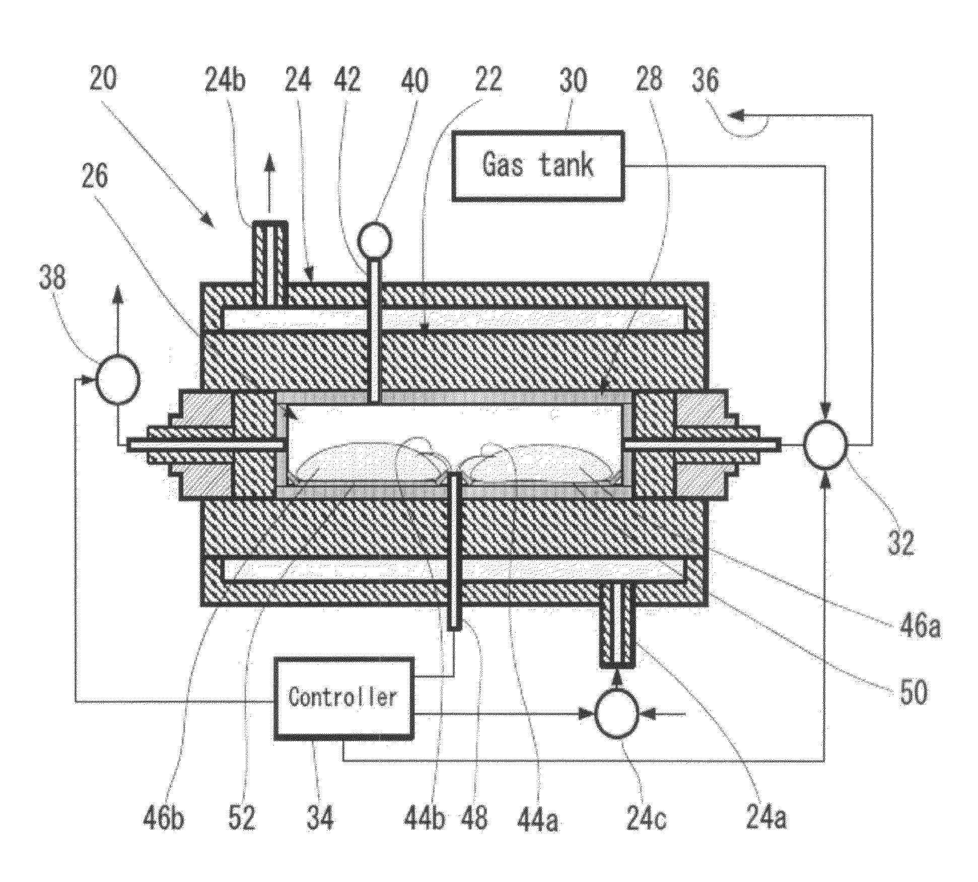
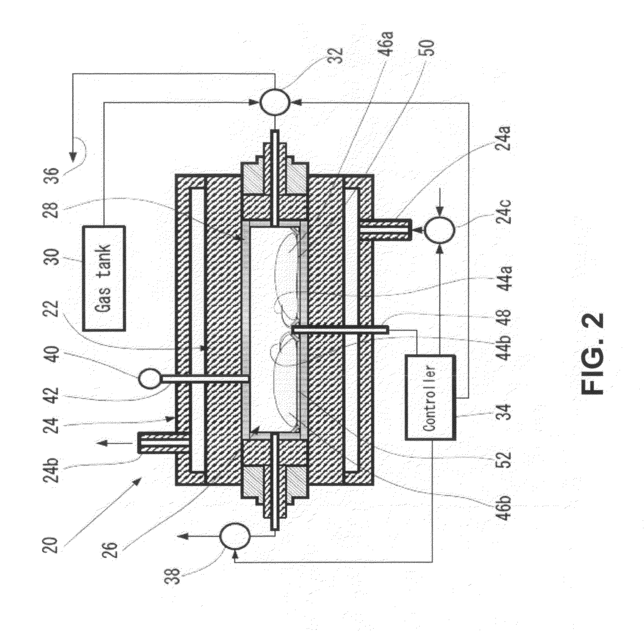
TermDescriptionArrested reduction-typeSynthesis using metal-I (or nonmetal) oxide and reducingcombustion synthesismetal-II to produce metal-I (or nonmetal) through combustionreaction, after which the product is quenched (cooled) at anappropriate rateHigh-surface-areaSpecific surface area exceeding 100 m2 / gpowderNanopowderParticle size less than or equal to 100 nmGreen mixtureInitial untreated mixture of reactant powdersInert gasNoble gas such as helium, neon, argon, krypton, xenon, as wellas any gas that is nonreactive under the conditions in which themethod of the present invention is carried out with materialsthat react with each other to form a particular compoundAmbient gas pressureInitial gas pressure contained in a reaction chamber around areaction-media sampleLocally initiatedReaction initiated in a discrete location (approximately areactionvolume of 1 mm3) on or within a...
PUM
| Property | Measurement | Unit |
|---|---|---|
| particle size | aaaaa | aaaaa |
| pressure | aaaaa | aaaaa |
| temperature | aaaaa | aaaaa |
Abstract
Description
Claims
Application Information