

Aqueous-based method of forming semiconductor film and photovoltaic device including the film
a technology of semiconductor film and film, applied in the field of kesterite film depositing method, can solve the problems of pure hydrazine vapor, high cost vacuum-based method, and at best 6.7 percent efficiency, and achieve the effect of improving safety and handling characteristics, reducing the risk of contamination, and improving the rheological and film-forming characteristics
- Summary
- Abstract
- Description
- Claims
- Application Information
AI Technical Summary
Benefits of technology
Problems solved by technology
Method used
Image

Examples
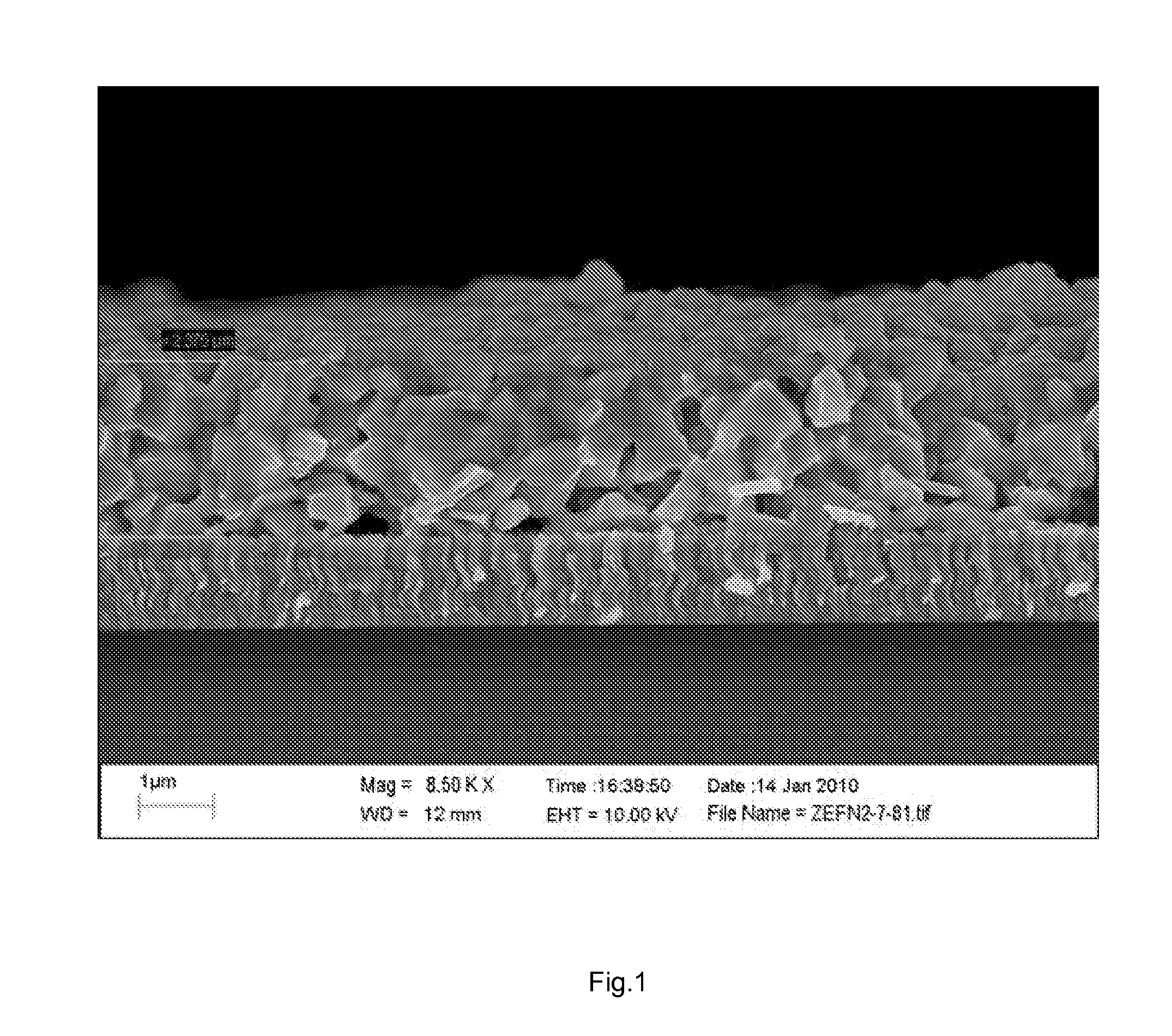
example 1
[0045]Preparation of aqueous ammonia dispersions by diluting pure hydrazine dispersions
[0046]All operations were performed in a nitrogen-filled glove box. The deposition solution was prepared in two parts in glass vials under magnetic stirring: A1, by dissolving Cu2S, 0.573 g and sulfur, 0.232 g in 3 ml of hydrazine and B1, by mixing SnSe, 0.790 g, Se, 1.736 g and Zn, 0.32 g with 7 ml of hydrazine. After 3 days under magnetic stirring, solution Al had an orange transparent aspect, while B1 was dark green and opaque. Solutions Al and dispersion B1 were mixed (C1) under magnetic stirring for 4 hours. 2 ml of dispersion C1 were mixed with 2 ml of 25% aqueous ammonia (ammonium hydroxide) to form dispersion D1.
[0047]Films of dispersion D1 were deposited on soda lime glass substrates coated with 700-1000 nm of molybdenum by spin coating at 800 rpm and heated preferably in a tubular oven or on a covered hot plate at about 425° C. for about 1 minute. The coating and heating cycle was repeat...
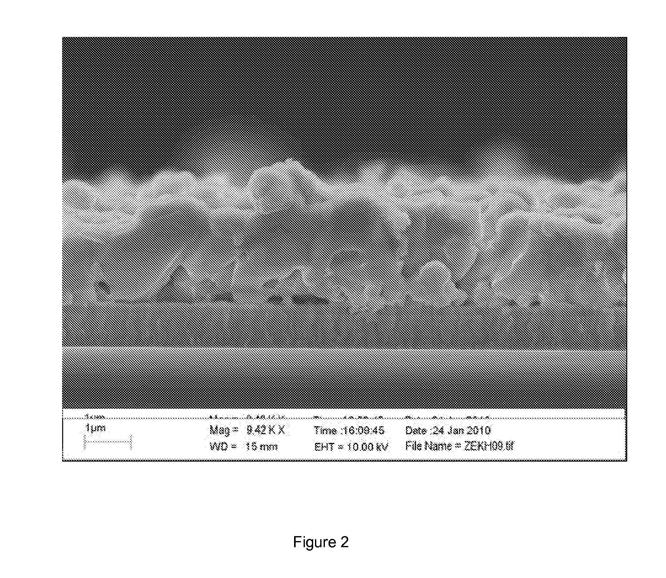
example 2
[0053]Preparation of aqueous hydrazine-hydrate dispersions by diluting hydrazine dispersion with water.
[0054]Procedures were identical to Example 1 with the difference that, instead of ammonium hydroxide, 1 ml of water was mixed with 2 ml of the dispersion C1. Total area device photovoltaic efficiency under simulated 1.5 AM illumination was 6.35%, with Voc=452 mV, Jsc=27 mA / cm2and FF=51% (Device cross section shown in FIG. 2).
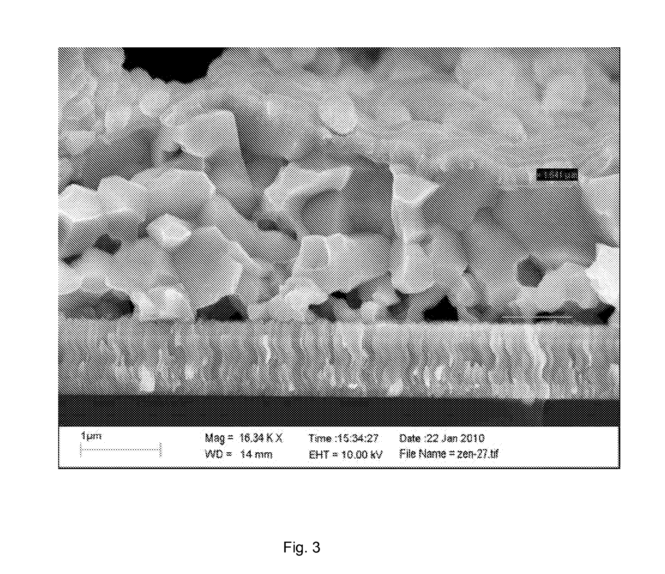
example 3
[0055]Preparation of inks without using pure hydrazine as intermediate solvent
[0056]Procedures were identical to Example 1 with the difference that, instead of pure hydrazine being used as the initial solvent, ammonium hydroxide (aqueous ammonia 25%) solution was premixed with equal volume of hydrazine and further used as a principal solvent (Solvent S3). Half of the amount of each solid indicated in Example 1 was digested in respective dispersions A3 and B3 by the addition of 2.5 and 5 ml of solvent S3, respectively.
[0057]Total area device photovoltaic efficiency under simulated 1.5 AM illumination was 4.52%, with Voc=441 mV, Jsc=22 mA / cm2 and FF=46%.
[0058]Layer uniformity observed by SEM (FIG. 3) requires further optimization which is expected to lead to significantly improved device parameters and result in efficiencies comparable to that of the pure hydrazine route.
PUM
| Property | Measurement | Unit |
|---|---|---|
| Temperature | aaaaa | aaaaa |
| Temperature | aaaaa | aaaaa |
| Percent by mass | aaaaa | aaaaa |
Abstract
Description
Claims
Application Information