

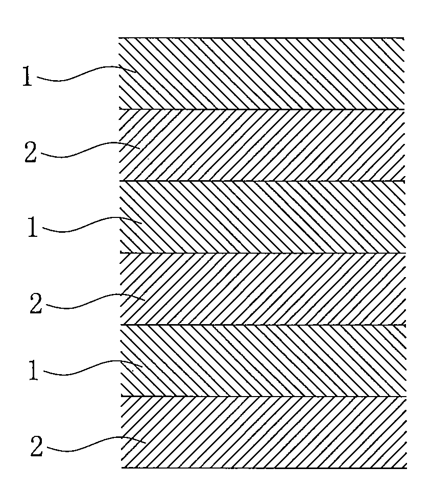
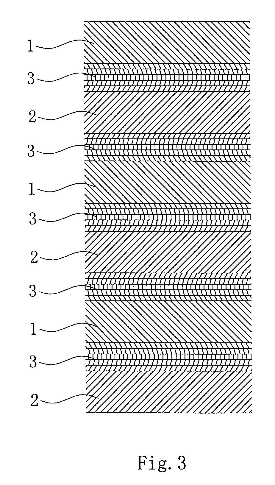
Thin film encapsulation method
a thin film, encapsulation technology, applied in the directions of organic semiconductor devices, semiconductor/solid-state device details, transportation and packaging, etc., can solve the problems of inefficiency, high cost, and limited encapsulation methods, so as to reduce the operative procedure, shorten the treatment cycle, and reduce the damage to the organic layer
- Summary
- Abstract
- Description
- Claims
- Application Information
AI Technical Summary
Benefits of technology
Problems solved by technology
Method used
Image

Examples
example 1
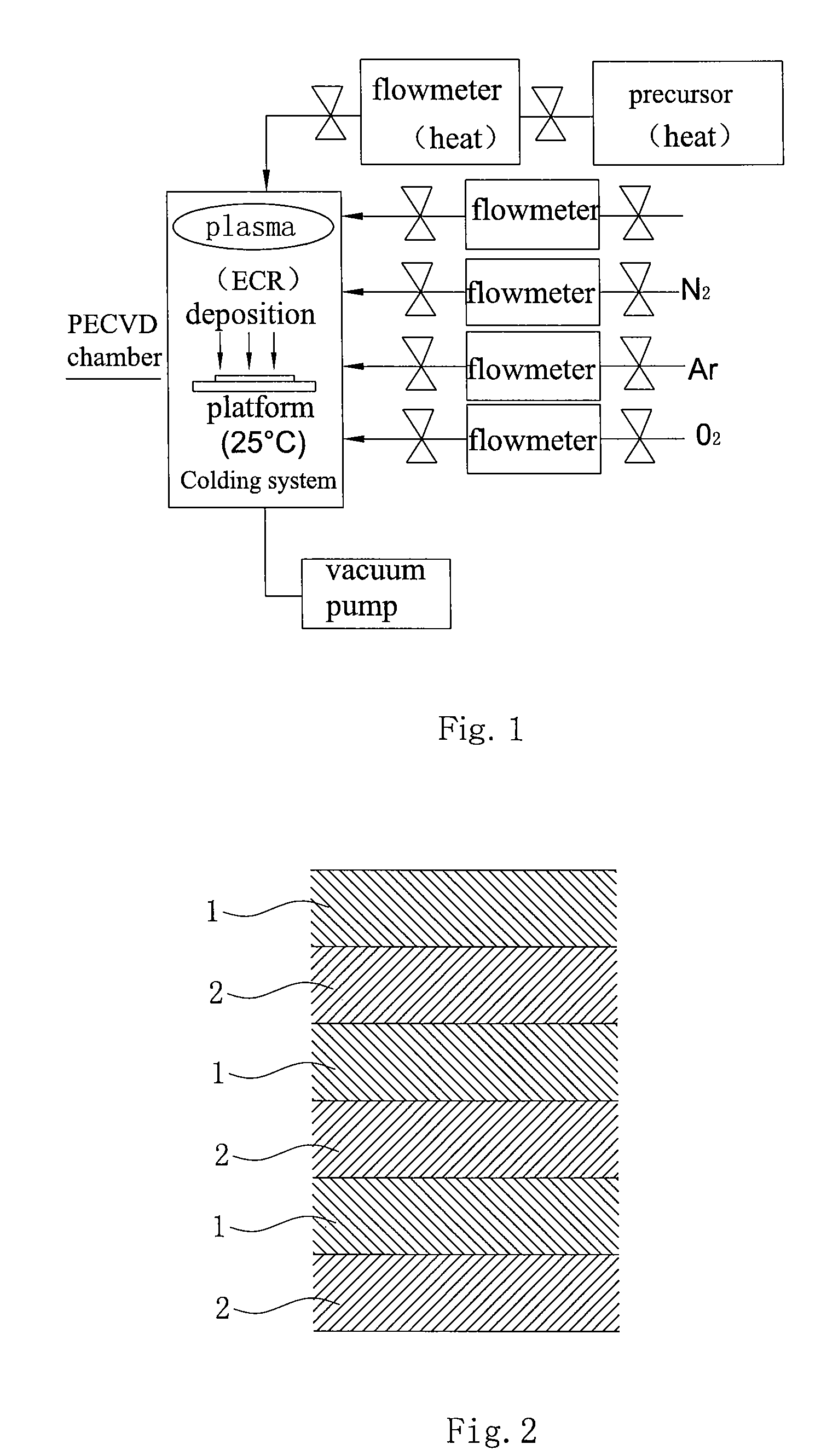
[0034]After the preparation of the OLED devices, firstly, in vacuum condition, deposit a 100 nm thick CuPc protection film on the aluminum electrode to prevent the devices from being harmed during the encapsulation. Then, transfer the OLED devices to the PECVD chamber (as FIG. 1) used for encapsulation without exposure to air. The diameter of the PECVD chamber is about 200 nm, cylindrical and 200 mm tall. The devices are placed on the rigid substrate upwards, and a mask is used to control the encapsulation area. Evacuate the cavity to 1.5 Pa and inject hexamethyldisiloxane (HMDSO), adjust the radio intensity to 60 mA under the plasma condition (electron cyclotron resonance, ECR, with the frequency of 40 KHz), and deposition the organic silicone polymer thin film under the Ar gas carrying condition for one minute with the internal pressure of 6 Pa. Next, turn off the plasma source, stop injecting Ar gas and inject oxygen to vary the internal pressure to 6 Pa. Turn on the plasma sourc...
example 2
[0035]Carry out the characterization test to the Alq3 OLED devices prepared on the ITO glass substrate encapsulated by applying the method described in Example 1, and compare it with the traditional glass covered epoxide resin encapsulation in lifetime and efficiency, the result shows that: the devices encapsulated with this method have almost the same efficiency to epoxide resin encapsulated devices, which reveals that this encapsulation is harmless to the devices performance. If there is no CuPc layer deposition before the OLED encapsulation, it will be slightly harmful. As for the lifetime test, the lifetime of the glass encapsulation component is 3000 h, while the lifetime of component in this invention exceeds 3000 h. This illustrates that this invention has the generally equal water and oxygen isolation capability to the glass covered epoxide resin encapsulation.
example 3
[0036]After finishing the preparation of the OLED devices in vacuum condition, deposit a 100 nm thick CuPc protection film on the aluminum electrode to prevent the devices from being harmed during the encapsulation. Then, transfer the OLED devices to the PECVD chamber used for encapsulation in the inert atmosphere. A mask is used to control the encapsulation area. Meanwhile, place a 1 μm thick thin steel plate beside the devices in order to grow the completely same encapsulation thin film on the steel plate while encapsulating the devices. Pump the chamber to 1.5 Pa and inject hexamethyldisiloxane (HMDSO), adjust the radio intensity to 60 mA under the plasma condition (electron cyclotron resonance, ECR, with the frequency of 40 KHz), and grow the organic silicon polymer thin film under the Ar gas carrying condition for one minute with the internal pressure of 8 Pa. Then, increase the NH3 gas gradually as 50 SCCM every 5 seconds to 200 SCCM and decrease the Ar flow as 50 SCCM every 5...
PUM
| Property | Measurement | Unit |
|---|---|---|
| thick | aaaaa | aaaaa |
| thickness | aaaaa | aaaaa |
| thickness | aaaaa | aaaaa |
Abstract
Description
Claims
Application Information