Nanostructures having high performance thermoelectric properties

a technology of nanostructures and thermoelectric properties, applied in the field of nanostructures, can solve problems such as increasing zt>1, and achieve the effect of decreasing the temperature of a locality

Inactive Publication Date: 2011-05-19
RGT UNIV OF CALIFORNIA
View PDF8 Cites 42 Cited by
  • Summary
  • Abstract
  • Description
  • Claims
  • Application Information

AI Technical Summary

Benefits of technology

[0010]The invention also provides for a method of decreasing the temperature of a locality comprising providing a device of the present invention, and applying an electric current through the...

Problems solved by technology

Over the past five decades, however, it has been challenging to ...

Method used


Image

  • Nanostructures having high performance thermoelectric properties
  • Nanostructures having high performance thermoelectric properties
  • Nanostructures having high performance thermoelectric properties

Examples


example 1

Rough Silicon Nanowire

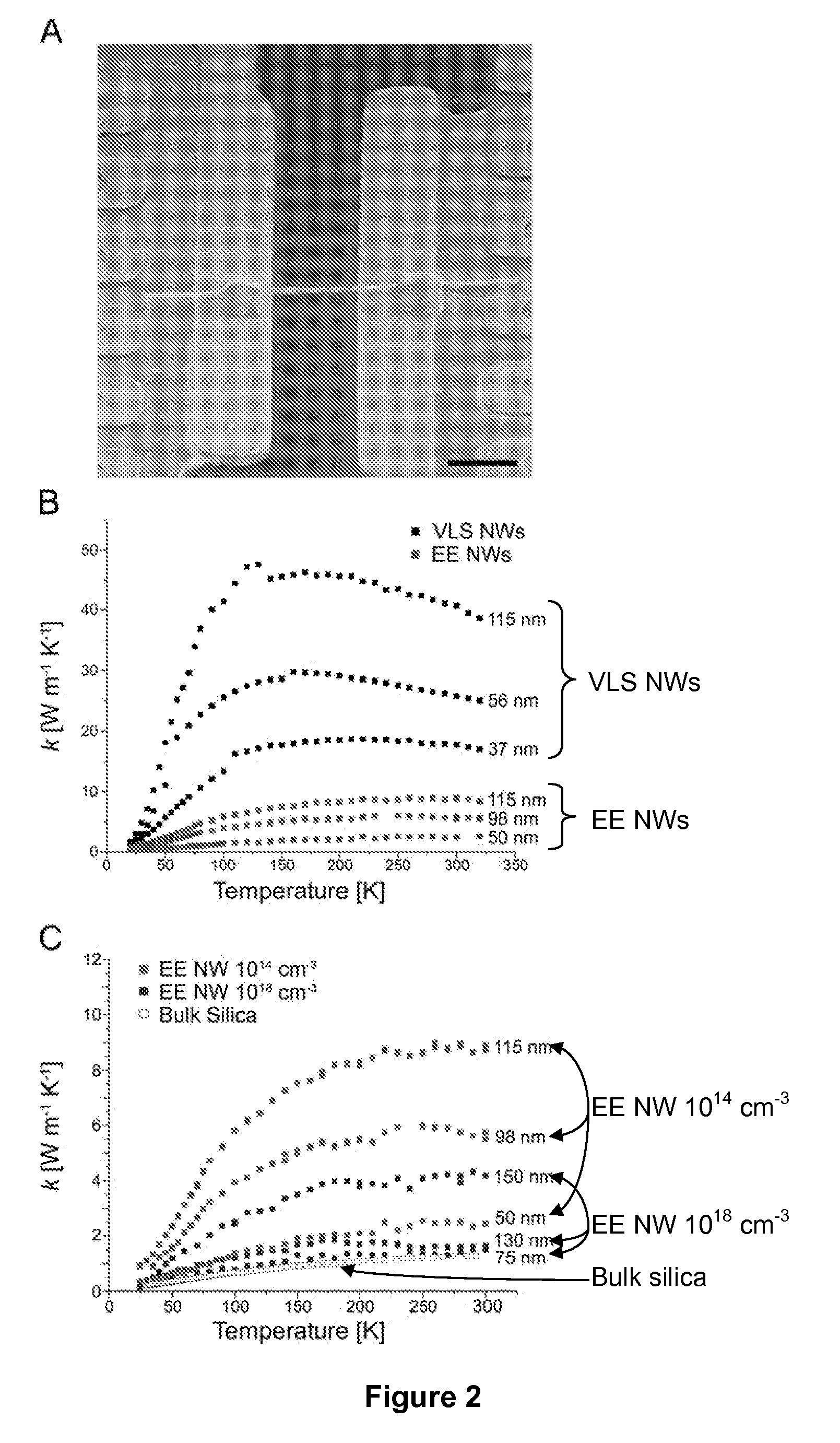
[0069]The most widely used commercial thermoelectric material is bulk Bi2Te3 and its alloys with Sb, Se, etc, which have ZT ˜1. While it is difficult to scale bulk Bi2Te3 to large-scale energy conversion, fabricating synthetic nanostructures for this purpose is even more difficult and expensive. Si, on the other hand, is the most abundant and widely used semiconductor with a large industrial infrastructure for low-cost and high-yield processing. Bulk Si, however, has a high k (˜150 W·m−1·K−1 at room temperature) (Touloukian, Y. S., Powell, R. W., Ho, C. Y. & Klemens, P. G. Thermal Conductivity: Metallic Elements and Alloys, Thermophysical Properties of Matter, v. 1, IFI / Plenum, New York, 339 (1970)), making the ZT ˜0.009 at 300 K (Weber, L. & Gmelin, E. Transport properties of silicon. Appl. Phys. A 53, 136-140 (1991), which are hereby incorporated by reference in their entireties). The spectral distribution of phonons contributing to the k of Si at room temper...

example 2

[0079]Nanowire synthesis. The standard nanowire synthesis was conducted on B-doped p-type (100) Si wafers. Wafer chips were sonicated in acetone and 2-propanol, and then put in a Teflon-lined autoclave in aqueous solution of 0.02 M AgNO3 and 5 M hydrofluoric acid (HF). The autoclave was sealed and placed in an oven at 50° C. for one hour. For 150 μm-long nanowires, wafer chips were prepared in the same fashion, and placed in the autoclave with 0.04 M AgNO3 and 5 M HF for four hours. Nanowires were also etched from entire Si wafers. Wafers were cleaned and placed in a Teflon dish with an identical etching solution and the synthesis ran at room temperature. The wafers etched in the open dish at room temperature produced wires similar to those etched in the autoclave but <50 μm in length. The same reaction conditions were used on wafers of all orientations, dopant type and concentration. Small regions on all samples had nanowires etched at an angle to normal.

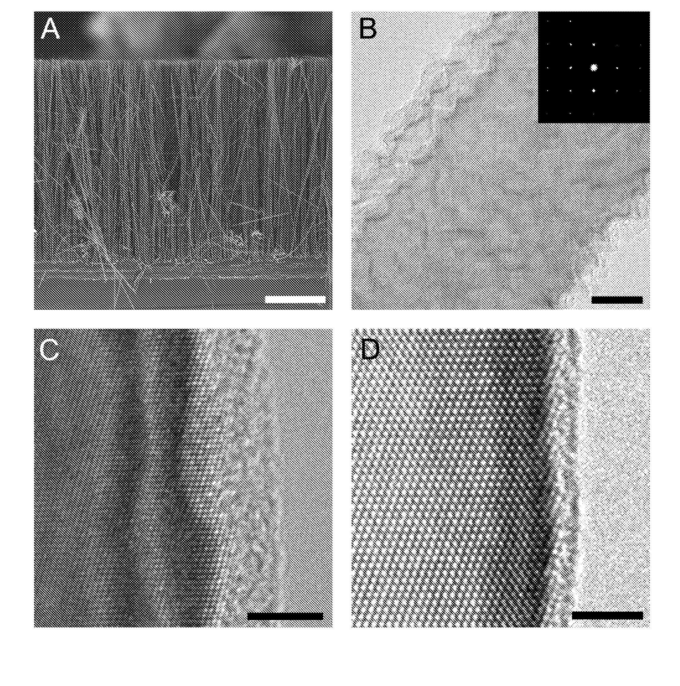
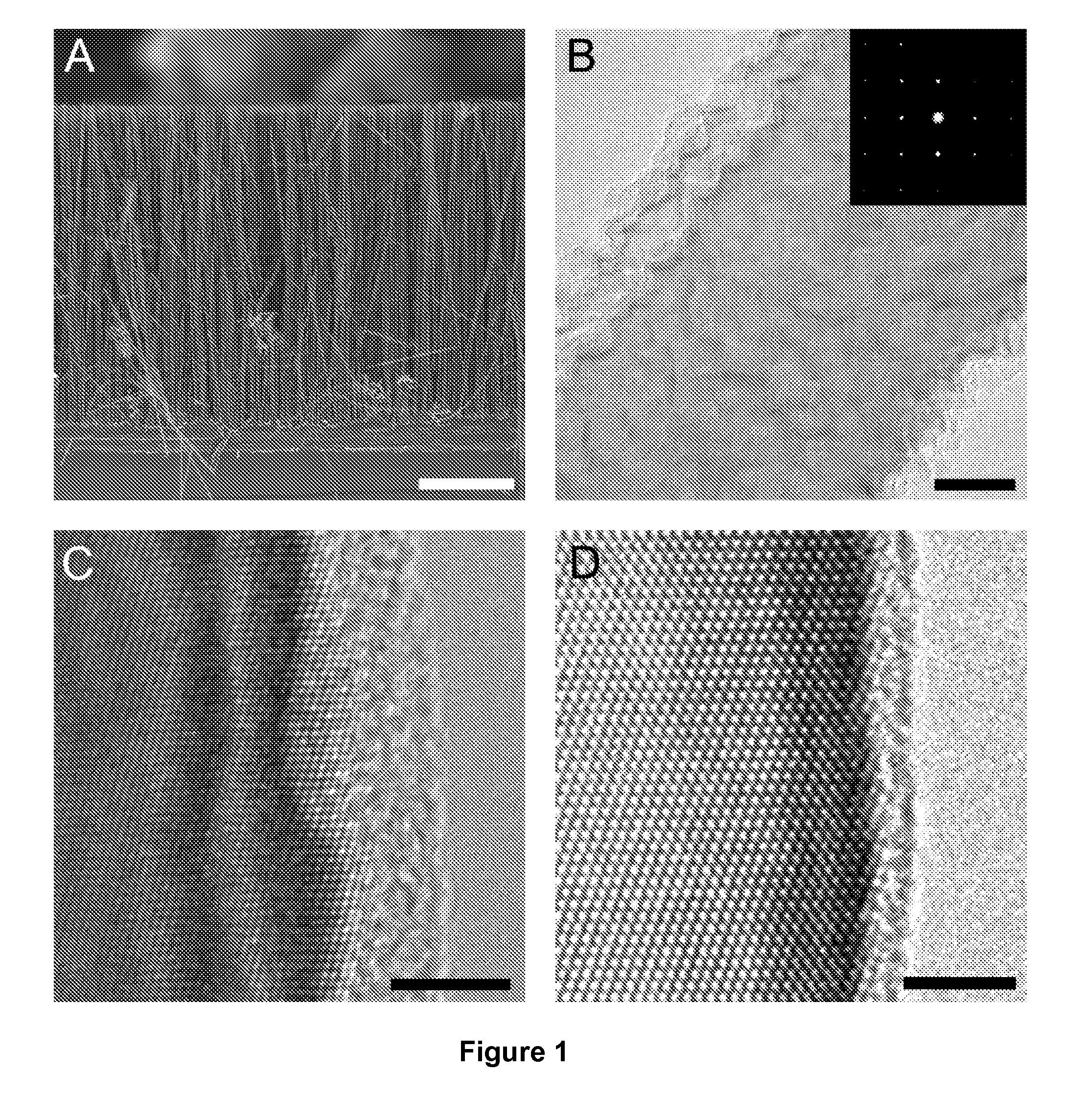
[0080]Nanowire characteriza...


PUM


Abstract

The invention provides for a nanostructure, or an array of such nanostructures, each comprising a rough surface, and a doped or undoped semiconductor. The nanostructure is an one-dimensional (1-D) nanostructure, such a nanowire, or a two-dimensional (2-D) nanostructure. The nanostructure can be placed between two electrodes and used for thermoelectric power generation or thermoelectric cooling.

Description

STATEMENT OF GOVERNMENTAL SUPPORT[0001]The invention described and claimed herein was made in part utilizing funds supplied by the U.S. Department of Energy under Contract No. DE-AC02-05CH11231. The government has certain rights in this invention.FIELD OF THE INVENTION[0002]This invention relates generally to nanostructures.BACKGROUND OF THE INVENTION[0003]Currently, approximately 90 percent of the world's power (˜1013 Watts or 10 TW) is generated by heat engines that use fossil fuel combustion as a heat source and typically operate at 30-40 percent efficiency, such that roughly 15 TW of heat is lost to the environment. Thermoelectric modules can potentially convert this low-grade waste heat to electricity, which could result in significant fuel savings and reduction in carbon emissions. Their efficiency depends on the thermoelectric figure of merit (ZT) of their material components, which is defined as ZT=S2σT / k where S, σ, k, and T are the Seebeck coefficient, electrical conductiv...

Claims


Application Information

Patent Timeline
IPC IPC(8): H01L35/28H01L29/06H01L35/30B82Y40/00
CPCH01L35/22H01L35/32H01L35/26H10N10/855H10N10/857H10N10/17B82B1/00H10N10/80H10N10/85H10N10/852H10N10/13
Inventor YANG, PEIDONGMAJUMDAR, ARUNAVAHOCHBAUM, ALLON I.CHEN, RENKUNDELGADO, RAUL DIAZ
Owner RGT UNIV OF CALIFORNIA
Why Eureka
Try Eureka