Apparatus and method for low-k dielectric repair

a dielectric and low-k technology, applied in the field of semiconductor processing, can solve the problems of affecting the capacitance and leakage current of the film, and achieve the effect of reducing the capacitance and leakage curren

Inactive Publication Date: 2011-06-23
APPLIED MATERIALS INC
View PDF8 Cites 10 Cited by
  • Summary
  • Abstract
  • Description
  • Claims
  • Application Information

AI Technical Summary

Benefits of technology

[0006]Disclosed herein are embodiments of methods and a systems for integrated, in-vacuo low-k dielectric thin film repair with the ability to restore k-values (e.g., reduce k-values to an “as-deposited” level) of a low-k dielectric film increased as a result of exposing portions (e.g., sidewalls of a via made in the low-k dielectric thin film) to various plasma processes (e.g., halogen etching plasmas, oxidizing/reducing cleaning plasmas, etc.) performed by one or more chamber on a multi-chambered mainframe platform. More specifically, the methods and systems may replenish

Problems solved by technology

However, carbon depletion of these porous films during plasma etching and ashing processes is known to lead to subsequent moisture uptake which detrimentally increases the capacitance and leakage cur

Method used


Image

  • Apparatus and method for low-k dielectric repair
  • Apparatus and method for low-k dielectric repair
  • Apparatus and method for low-k dielectric repair

Examples


Embodiment Construction

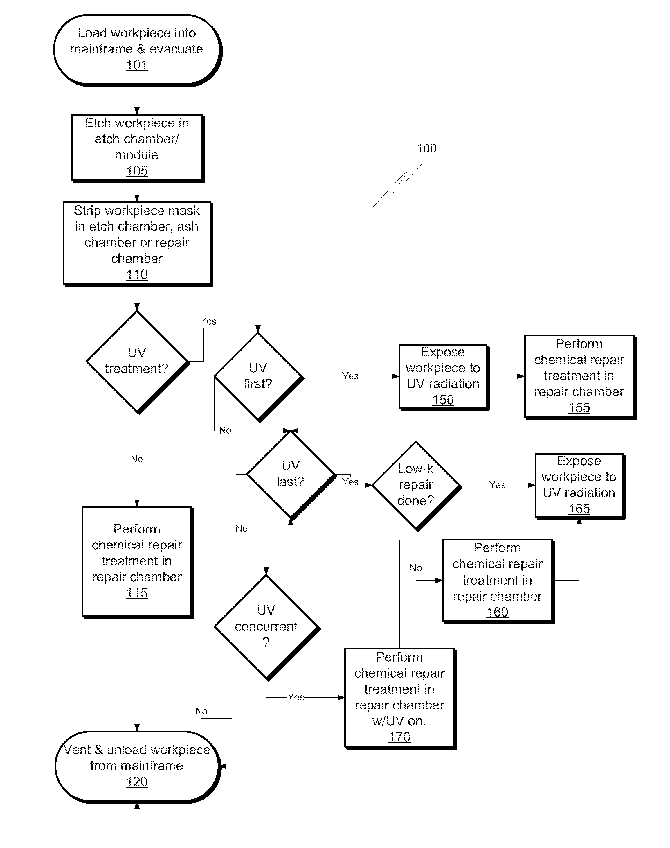
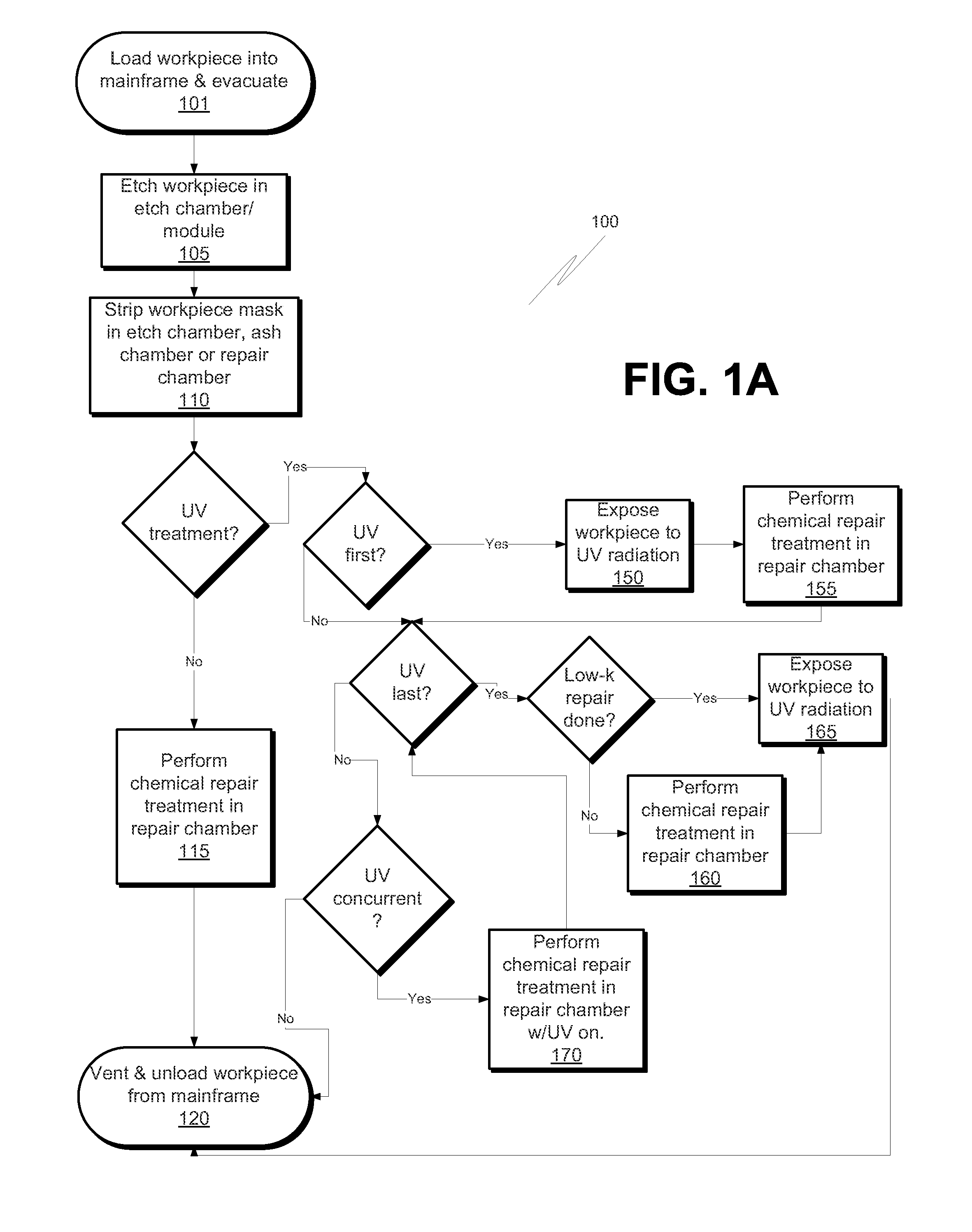
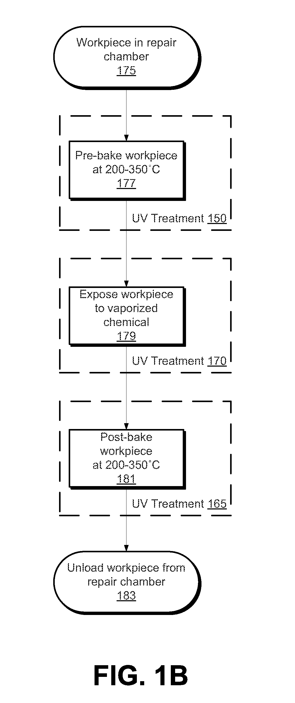
[0024]Embodiments of systems and methods for repair of low-k, porous, silicon-based dielectric thin films are described herein. In the following description, numerous specific details are set forth, such as order of operations, in order to provide a thorough understanding of the present invention. It will be apparent to one skilled in the art that the present invention may be practiced without these specific details. In other instances, well-known features, such as specific process recipes and equipment components, are not described in detail in order to not unnecessarily obscure the present invention. Furthermore, it is to be understood that the various embodiments shown in the Figures are merely illustrative representations and are not necessarily drawn to scale.

[0025]The extent of such carbon incorporation / repair of a low-k film may be characterized through electron energy loss spectroscopy (EELS), transmission electron microscopy (TEM), electrical capacitance and leakage measure...


PUM

PropertyMeasurementUnit
Temperatureaaaaaaaaaa

Abstract

A method, a system and a computer readable medium for integrated in-vacuo repair of low-k dielectric thin films damaged by etch and/or strip processing. A repair chamber is integrated onto a same platform as a plasma etch and/or strip chamber to repair a low-k dielectric thin film without breaking vacuum between the damage event and the repair event. UV radiation may be provided on the integrated etch/repair platform in any combination of before, after, or during the low-k repair treatment to increase efficacy of the repair treatment and/or stability of repair.

Description

CLAIM OF PRIORITY[0001]This application is related to, and claims priority to, the provisional utility application entitled “APPARATUS AND METHOD FOR LOW-K DIELECTRIC REPAIR,” filed on Aug. 5, 2009, having an application number of 61 / 231,653 and herein incorporated by reference in its entirety for all purposes.BACKGROUND[0002]1) Field[0003]The invention is in the field of Semiconductor Processing and more particularly relate to repair of low-k / ultra low-k dielectric materials which have been damaged by prior plasma processing.[0004]2) Description of Related Art[0005]Dielectric materials with an effective dielectric constant (k) below about 2.5, commonly referred to as “ultra low-k” materials, become extremely important to integrated circuit performance beyond the 45 nm technology node. Generally, these ultra low-k materials, referred to herein as simply “low-k,” have increased porosity relative to materials having a k-value in the 2.5 to 3.0 range. However, carbon depletion of these...

Claims


Application Information

Patent Timeline
IPC IPC(8): H01L21/00C23C16/50H01L21/465
CPCH01L21/3105H01L21/31058H01L21/67167H01L21/76831H01L21/67207H01L21/76814H01L21/76825H01L21/6719
Inventor CARDUCCI, JAMES D.NEMANI, SRINIVAS D.TANG, HAIRONGSUN, HUIMARKOVSKY, IGORGOLD, EZRA R.KAYA, IWALANI S.YIEH, ELLIE Y.ZHANG, CHUNLEICOLLINS, KENNETH S.ARMACOST, MICHAEL D.BALAKRISHNA, AJITLILL, THORSTEN B.
Owner APPLIED MATERIALS INC
Why Eureka
Try Eureka