
Method for producing microstructured templates and their use in providing pinning enhancements in superconducting films deposited thereon

a microstructured template and enhancement technology, applied in the direction of superconductor films, vacuum evaporation coatings, superconductor devices, etc., can solve the problems of superconductor films, unacceptably low critical current densities of hts tapes, and dispersion of critical current density, so as to increase flux pinning and reduce ac losses. , the effect of industrial efficiency and financial feasibility

Active Publication Date: 2011-06-30
UNIV OF TENNESSEE RES FOUND +1
View PDF26 Cites 26 Cited by
  • Summary
  • Abstract
  • Description
  • Claims
  • Application Information

AI Technical Summary

Benefits of technology

[0010]The invention advantageously provides an industrially efficient and financially feasible method for incorporating nanoscale defects and / or filamentized features into superconducting films, tapes, and wires. By this method, superconducting tapes with increased flux pinning and reduced AC losses can be made cost-effectively and efficiently on an industrial scale, thereby making superconducting tapes and wires a more realistic option as wiring in commonplace applications. The method also makes possible the ability to modulate the level of AC loss reduction, flux pinning, and other attributes of the superconducting film by appropriate modification of the phase-separated layer by judicious selection or optimization of sputtering and related conditions.

Problems solved by technology

The first HTS tapes suffered from unacceptably low critical current densities, a problem caused by poor alignment of grains in the HTS film or coating with grains of the substrate.
However, a well-known problem of HTS tapes and wires to which much research has been directed is the dissipation in critical current density (typically expressed as Jc) of the superconductor film when the superconductor film is exposed to an external magnetic field.
The pinning defects have been found to significantly reduce current density losses in superconductor films in the presence of an external magnetic field.
However, the common techniques currently capable of producing such phase-separated substrates (e.g., physical vapor deposition (PVD), pulsed laser deposition (PLD), molecular beam epitaxy (MBE), and atomic layer deposition (ALD)), possess the significant drawbacks of being non-scalable, cost prohibitive, and industrially inefficient (i.e., typically of low throughput).

Method used


Image

  • Method for producing microstructured templates and their use in providing pinning enhancements in superconducting films deposited thereon
  • Method for producing microstructured templates and their use in providing pinning enhancements in superconducting films deposited thereon
  • Method for producing microstructured templates and their use in providing pinning enhancements in superconducting films deposited thereon

Examples


example 1

The Substrates

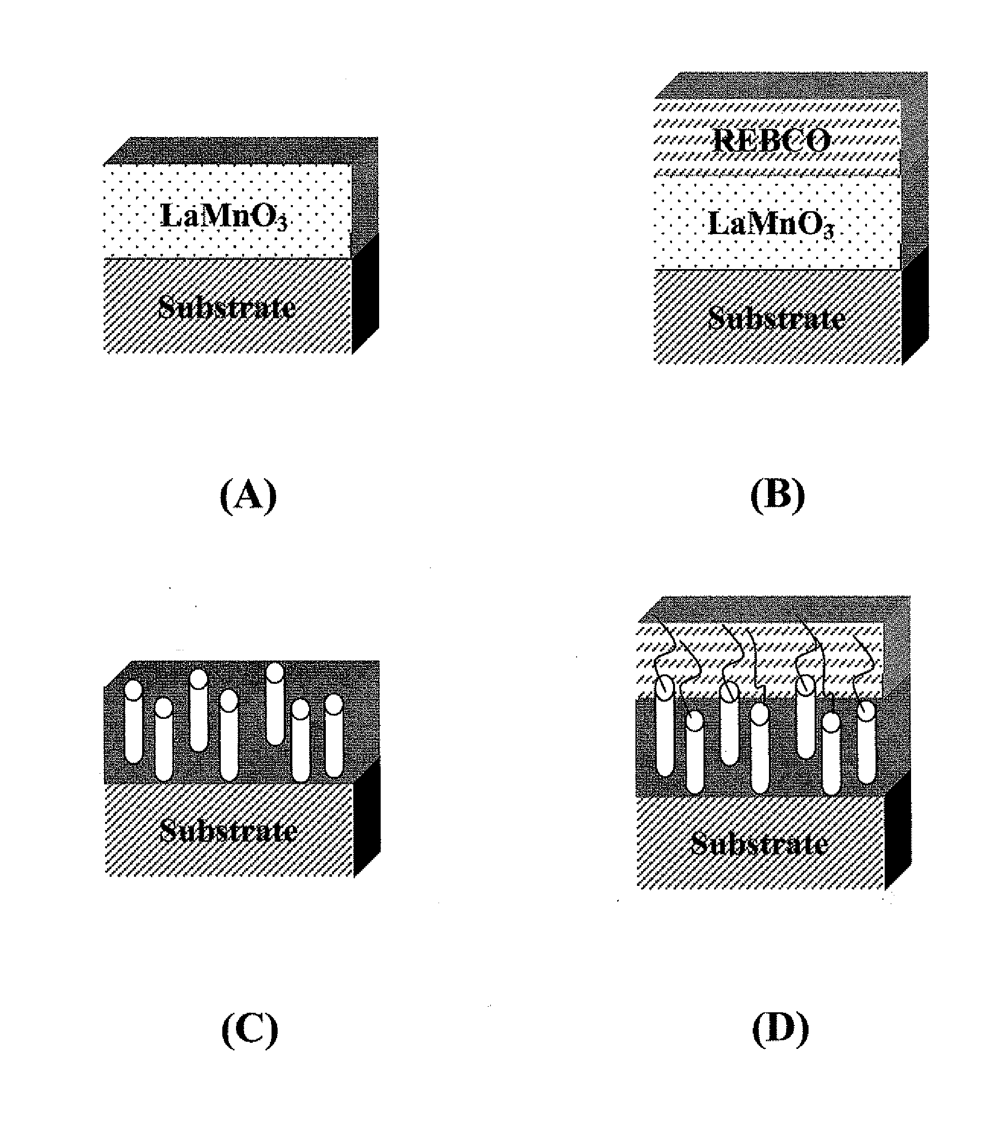
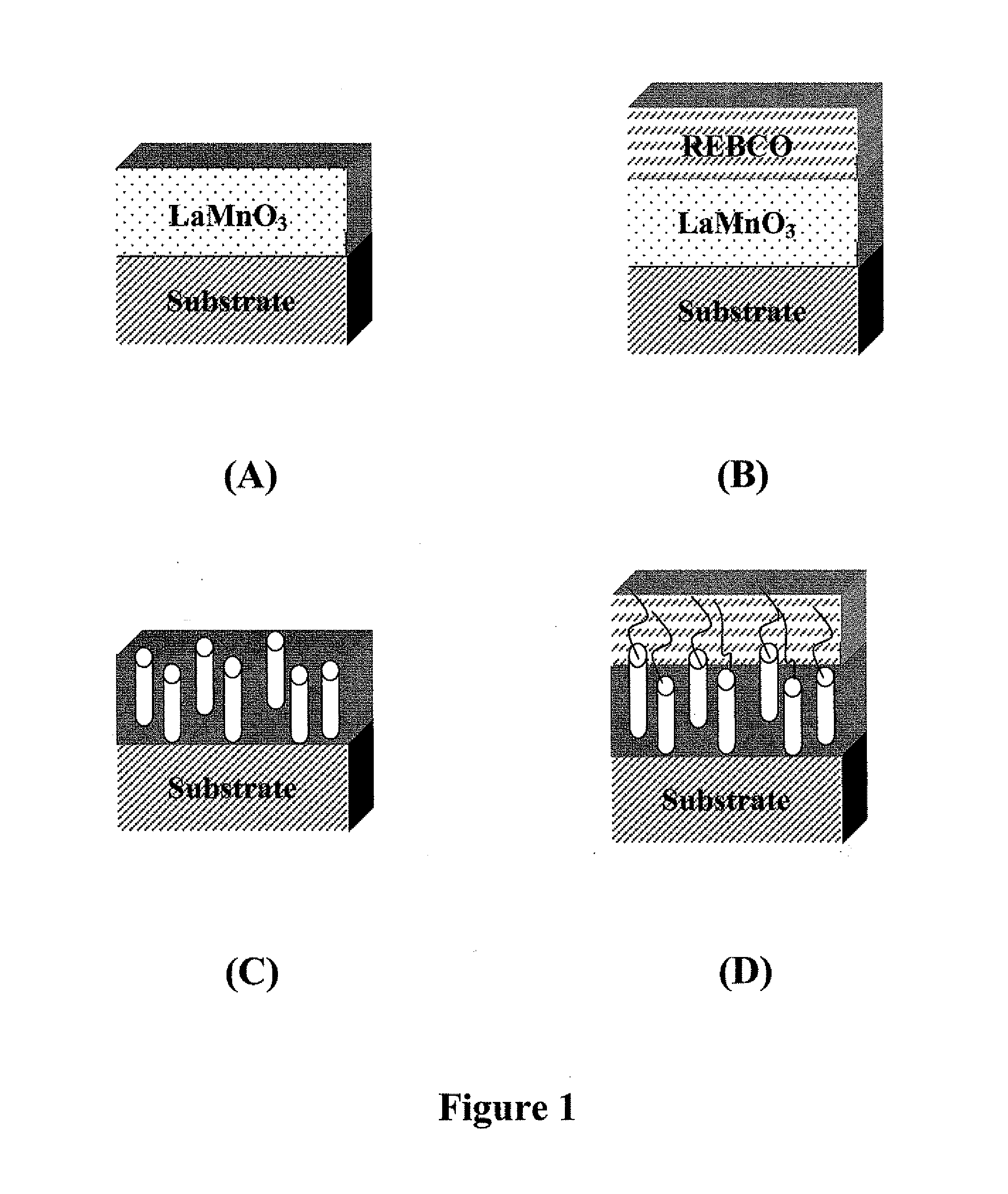
[0126]RF magnetron sputtering was employed to deposit phase-separated layers on two types of substrates referred to herein as “IBAD-MgO” and “Homo-epi-MgO / IBAD-MgO” substrates or templates. The substrate referred to as “IBAD-MgO” refers to the IBAD-MgO / Y2O3 / Al2O3 / Ni-based alloy substrate as generally depicted in FIG. 10B. The substrate referred to as “Homo-epi-MgO / IBAD-MgO” refers to the Homo-epi-MgO / IBAD-MgO / Y2O3 / Al2O3 / Ni-based alloy substrate as generally depicted in FIG. 1A. The substrates used in this study were fabricated according to the method described in X. M. Xiong, et al., “High Throughput Processing of Long-length IBAD MgO and Epi-buffer Templates at SuperPower”, IEEE Trans. Appl. Supercond., 17, 3375 (2007).

IBAD-MgO Substrate

[0127]The first layer is an 80 nm-thick Al2O3 layer that serves as a barrier for upward diffusion of substrate cations. The superior diffusion barrier properties of Al2O3 for transition metals such as Ni, Cr, Mn, Mo, etc., as well as f...

example 2

Deposition of a Phase-Separated LMO:MgO Layer on IBAD-MgO and Homo-Epi-MgO / IBAD-MgO Substrates

In-Situ Annealing of Substrate Prior to Deposition of LMO:MgO Phase-Separated Layer

[0129]As the MgO surface is known to be hygroscopic, an annealing process was performed on the substrate of the MgO surface prior to deposition of the phase-separated layer. The annealing process was conducted in a manner that removes surface-adsorbed water and hydrocarbons. Removal of these species ensures a chemically clean surface for the reproducible growth of subsequent LMO:MgO composite layers. The annealing process included the following steps:

[0130]1. The annealing gas, in this case, a mixture of Ar, H2 (4%) and O2 (or alternatively, a mixture of Ar, H2 (4%) and water vapor) was introduced into the deposition chamber, and the total chamber pressure adjusted to 5×10⁻³ Torr.

[0131]2. The temperature of the substrates was increased from room temperature (RT) to 720° C. at a rate of 140° C. / min.

[0132]3. T...

example 3

Analysis of the Phase-Separated Layers in the LMO:MgO-Coated Substrates

X-Ray Diffraction Measurements

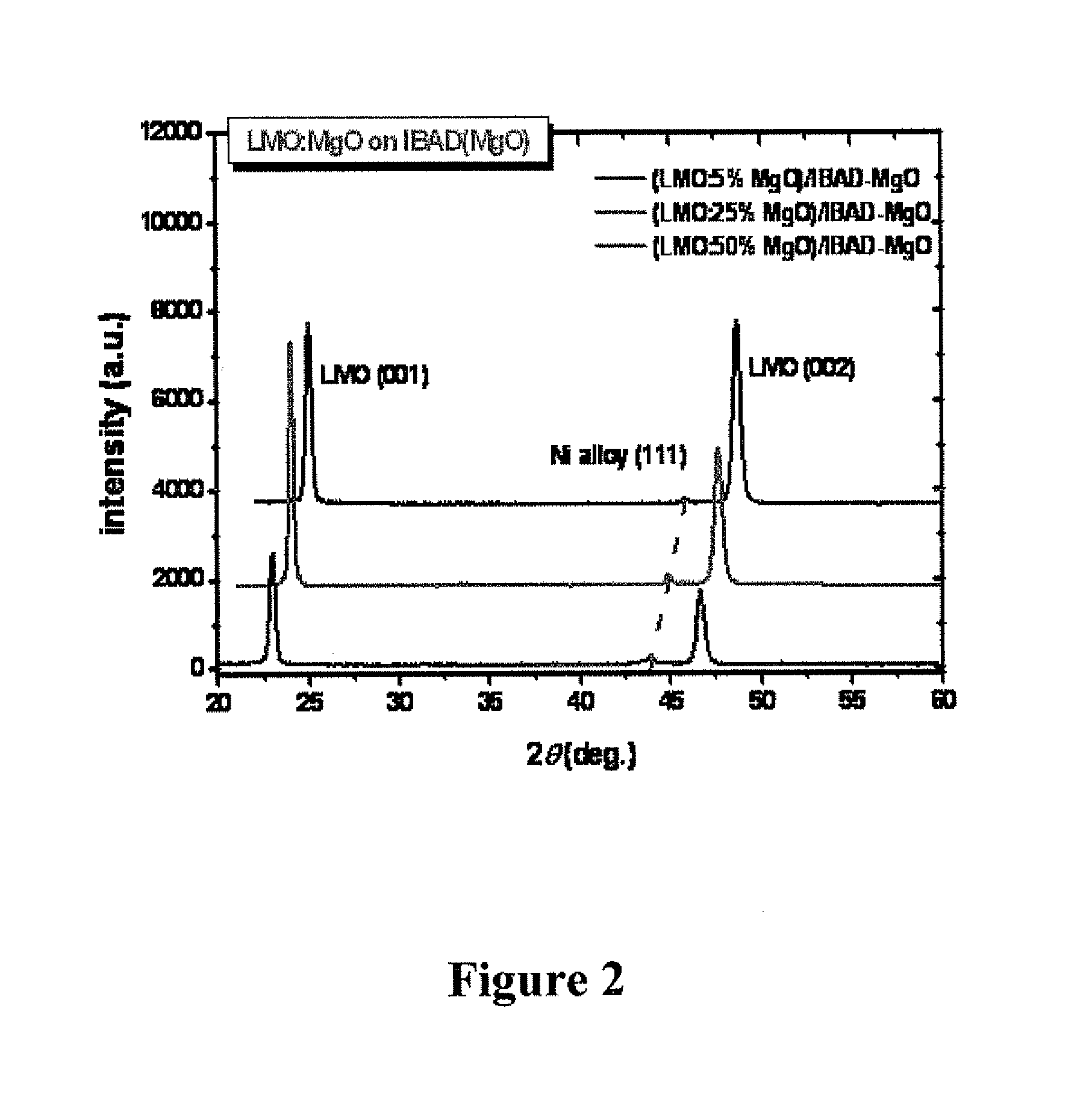
[0149]FIG. 2 shows a series of X-ray θ-2θ scans for LMO:MgO composite films, prepared above at varying MgO concentrations of 5 vol %, 25 vol %, and 50 vol %, deposited directly on IBAD-MgO templates. As shown, for all compositions, the films have a preferred c-axis orientation. Due to the absence of a homo-epi layer (the bottom scan) it is difficult to distinguish the MgO peak reflection at this level of display.

Atomic Force Microscopy

[0150]FIG. 3 shows the surface morphology of the composite LMO:MgO (25 vol %) film deposited on homo-epi-MgO / IBAD-MgO template (as prepared above) as obtained by an AFM scan. As shown, the AFM scan shows the presence of a high density of bright features. Significantly, a scanning Auger microprobe analysis of these features confirmed that these features are Mg-rich regions, and this evidences two-dimensional projections of phase-separated, vertically-ord...


PUM

PropertyMeasurementUnit
Temperatureaaaaaaaaaa
Compositionaaaaaaaaaa
Superconductivityaaaaaaaaaa

Abstract

The present invention relates to a method for producing a phase-separated layer useful as a flux pinning substrate for a superconducting film, wherein the method includes subjecting at least a first and a second target material to a sputtering deposition technique in order that a phase-separated layer is deposited epitaxially on a primary substrate containing an ordered surface layer. The invention is also directed to a method for producing a superconducting tape containing pinning defects therein by depositing a superconducting film on a phase-separated layer produced by the method described above.

Description

[0001]This invention was made with government support under Contract Number DE-AC05-00OR22725 between the United States Department of Energy and UT-Battelle, LLC. The U.S. government has certain rights in this invention.FIELD OF THE INVENTION[0002]The present invention relates to high temperature superconductor films, tapes, and wires, and more particularly, to such films, tapes, and wires with improved flux-pinning and reduced AC losses.BACKGROUND OF THE INVENTION[0003]Methods for the preparation of films of high temperature superconductor (HTS) materials on various substrates are well known. These methods have been instrumental for converting HTS materials into tapes and wires, a necessary step in the effort for integrating these materials as wiring into conventional electrical grid systems and devices. Several companies produce HTS wires and tapes of various lengths.[0004]The first HTS tapes suffered from unacceptably low critical current densities, a problem caused by poor align...

Claims


Application Information

Patent Timeline
IPC IPC(8): H01L39/24C23C14/34C23C14/35
CPCC23C14/024C23C14/08C23C14/35Y10T428/25H01L39/2483H01L39/2461C23C14/5806H10N60/0828H10N60/0632
Inventor AYTUG, TOLGAPARANTHAMAN, MARIAPPAN PARANSPOLAT, OZGUR
Owner UNIV OF TENNESSEE RES FOUND
Learn More