Sputtering target, method for forming amorphous oxide thin film using the same, and method for manufacturing thin film transistor

a technology of amorphous oxide and amorphous oxide, which is applied in the direction of diaphragms, metallic material coating processes, domestic applications, etc., can solve the problems of no disclosure of bulk resistance value, defects on the obtained film, and slow sputtering rate, so as to reduce the possibility of forming white spots and improve the sputtering effect. , the effect of good stability

Active Publication Date: 2011-07-21
IDEMITSU KOSAN CO LTD
View PDF7 Cites 28 Cited by
  • Summary
  • Abstract
  • Description
  • Claims
  • Application Information

AI Technical Summary

Benefits of technology

[0018]The present invention provides a sputtering target having properties such as good appearance with less possibility of forming White-spot, good stability in sputtering, reduced formation of particles (or dusts) of sputtering material during sputtering, and accelerated sputtering rate.
[0019]The present invention allows to form two kinds of homologous crystals simultaneously by the specific production method or the specific production conditions (such as sintering temperature or sintering time).
[0020]The present invention also provide a sputtering target comprising both an oxide crystal represented by InGaZnO4 and an oxide crystal represented by In2Ga2ZnO7, and then the present invention can solve the above-mentioned problems suitably.
[0021]The sputtering target of the present invention is used for producing semi-conductors to make an excellent oxide semi-conductors or TFTs.
[0022]A sputtering target of the present invention comprises an oxide sintered body containing two or more homologous crystal struc

Problems solved by technology

However, there is no disclosure about bulk resistance value, and there is a problem to use the compound for a sputtering target (Patent Document 4).
Furthermore, for example, a sputtering target comprised of indium oxide/gallium oxide/zinc oxide using the compound of InGaO3(ZnO)m (an oxide sintered body showing a crystalline structure of homologous phase) causes an abnormal electrical discharge by anomalous growth of the compound shown by InGaO3(ZnO)m during sputtering, and thus there was a problem about defects on the obtained film (see Patent Document 2)

Method used


Image

  • Sputtering target, method for forming amorphous oxide thin film using the same, and method for manufacturing thin film transistor
  • Sputtering target, method for forming amorphous oxide thin film using the same, and method for manufacturing thin film transistor
  • Sputtering target, method for forming amorphous oxide thin film using the same, and method for manufacturing thin film transistor

Examples


example 1

[0193]Each powder of In2O3 (made by Kojundo Chemical Laboratory, Co., 99.99% purity), Ga2O3 (made by Kojundo Chemical Laboratory, Co., 99.99% purity), and ZnO (made by Kojundo Chemical Laboratory, Co., 99.99% purity) was weighed to meet atom ratio of metals contained in a mixed powder being In:Ga:Zn=1:1:1. Each weighed powder was added to a 500 ml polyamide container, 200 g of zirconia beads having 2 mm in diameter were further added, ethanol was also added as a disperse media, and then wet-mixing was conducted using a planetary ball mill device provided by Fritz Japan for one hour. The obtained mixture was calcined in an alumina crucible under ambient pressure at 1000° C. for 5 hours, then unraveled using the planetary ball mill device again for 1 hour, and then obtained a ground, calcined product having an average diameter (JIS R 1619) of 3 μm. Thus prepared calcined product was formed in a disc configuration having 20 mm in diameter and 6 mm in thickness by a uniaxial pressing (1...

example 2

[0195]As crude powders, Indium oxide powder having 6 m2 / g of specific surface area, gallium oxide powder having 6 m2 / g of specific surface area, and zinc oxide powder having 5 m2 / g of specific surface area were weighed to meet mass ratio of 45:30:25. Further, Ge as a positive quadrivalent metal was added to be an amount of 500 ppm, and then mixed and ground using a wet-type medium agitating mill. Zirconia beads having 1 mmφ was used as a medium. Specific surface area of the ground powders was increased 2 m2 / g compared to that of the crude mixed powders. The obtained mixed powders were dried by using a spray dryer, then filled in a metal mold, and then press formed by a cold press device. Sintering was then conducted by flowing oxygen under oxygen atmosphere at 1500° C. for 2 hours. Based on the above steps, an oxide sintered body for a sputtering target having 6.2 g / cm2 of sintered body density was obtained without calcining step.

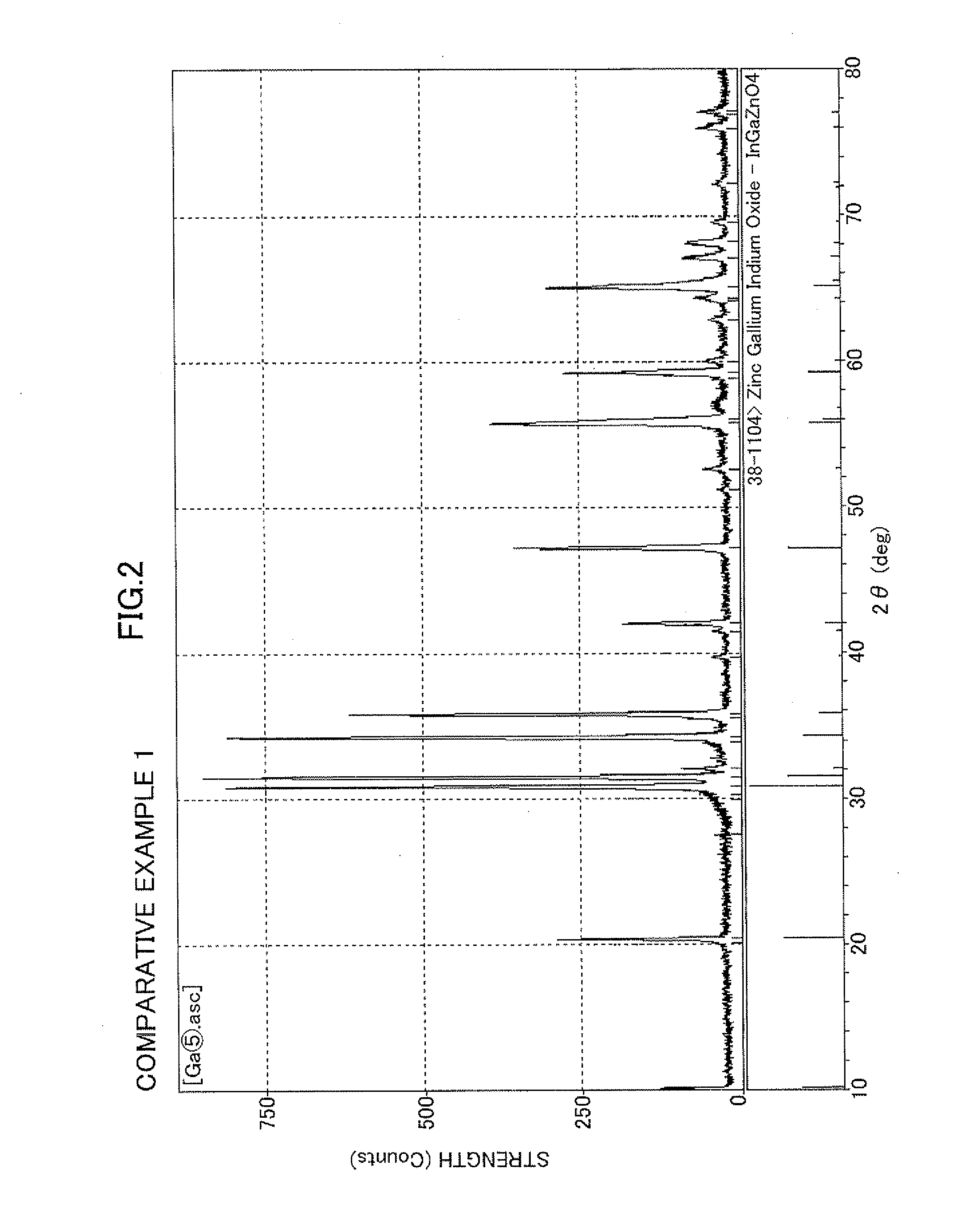
[0196]The obtained product was confirmed by X-ray dif...

example 3

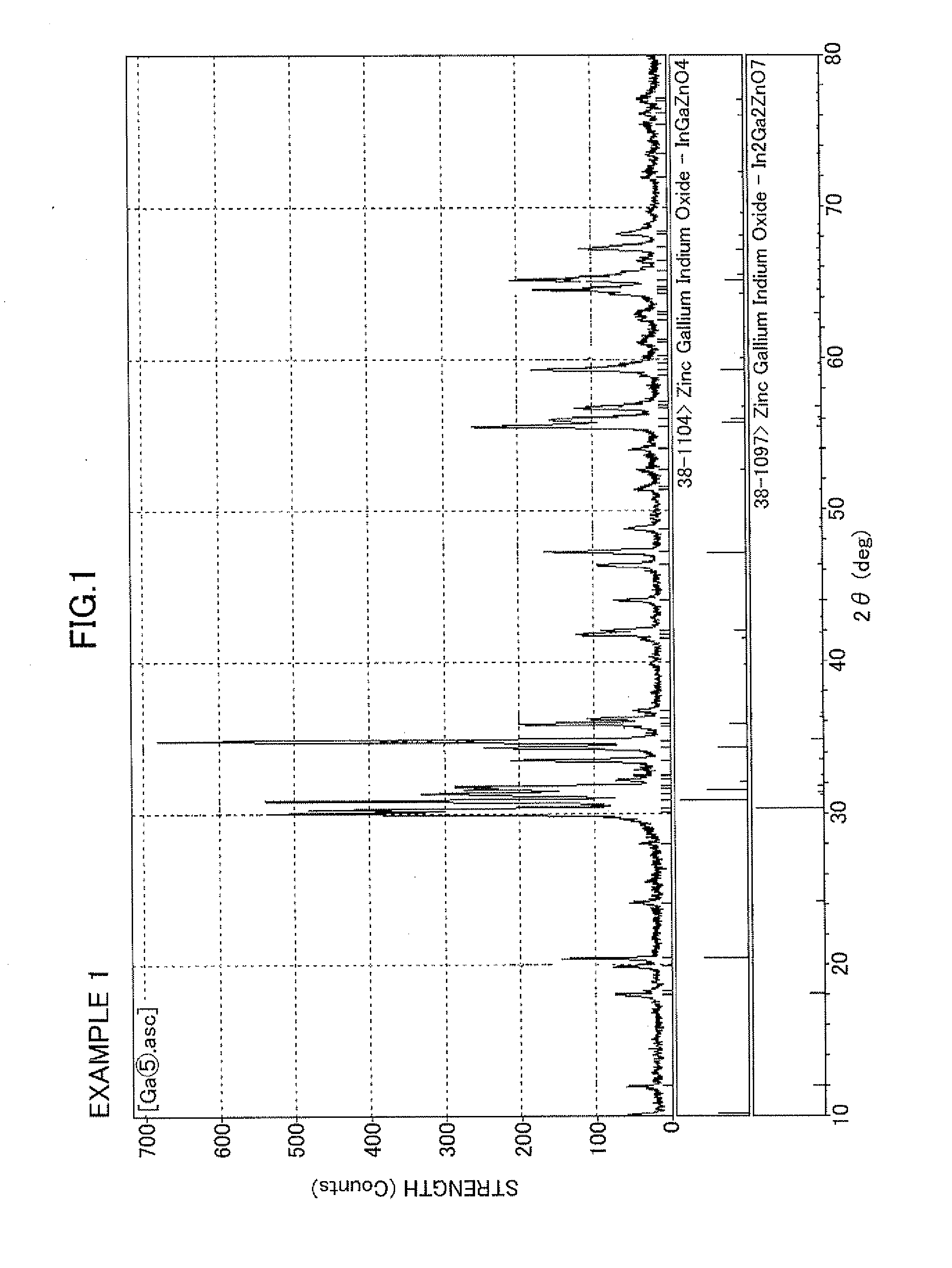
[0198]The same sintering process was conducted as that of Example 2 except that Sn was used in place of the quadrivalent or more metal.

[0199]Under X-ray diffraction, when the maximum peak strength for the oxide crystal represented by InGaZnO4 (JCPDS Card No. 38-1104) is P(1), and when the maximum peak strength for the oxide crystal represented by In2Ga2ZnO7 (JCPDS Card No. 38-1097) is P(2), the peak strength ratio P(1) / P(2) was 1.3. In addition, based on a shift of interstitial distance calculated from X-ray diffraction, and based on structural analysis using high brightness emitted light, it could be found that a part of In or Ga was replaced by Sn.


PUM

PropertyMeasurementUnit
Temperatureaaaaaaaaaa
Timeaaaaaaaaaa

Abstract

Disclosed is a sputtering target having a good appearance, which is free from white spots on the surface. The sputtering target is characterized by being composed of an oxide sintered body containing two or more kinds of homologous crystal structures.

Description

TECHNICAL FIELD[0001]The present invention relates to a sputtering target characterized by an oxide sintered body which comprises two or more homologous crystal structures, a method for forming an amorphous oxide thin film using the target, and a method for manufacturing a thin film transistor.BACKGROUND OF THE ART[0002]Oxide semiconductor films comprised of some metallic composite oxides have high mobility property and good optical transparency for visible light. Therefore, the films are used for variety of applications such as switching elements or drive circuit elements for a liquid crystal display device, a thin film electroluminescence display device, an electrophoresis method display device, and a powder transfer method display device. Especially, oxide semiconductor films comprising indium oxide / zinc oxide are brought to attention in light of their ease of manufacture, price, or outstanding properties. Specifically, oxides comprising indium oxide / gallium oxide / zinc oxide, or ...

Claims


Application Information

Patent Timeline
IPC IPC(8): H01L21/31C23C14/34C04B35/64
CPCB82Y30/00Y10T428/24355C04B35/44C04B35/453C04B35/645C04B2235/3217C04B2235/3224C04B2235/3244C04B2235/3272C04B2235/3286C04B2235/3287C04B2235/3293C04B2235/40C04B2235/404C04B2235/5409C04B2235/5436C04B2235/5445C04B2235/5454C04B2235/666C04B2235/725C04B2235/77C23C14/086C23C14/3414H01L21/02554H01L21/02565H01L21/02592H01L21/02631H01L29/7869H01L29/24H01L29/66969C04B35/2675H01L29/78693
Inventor YANO, KOKIKAWASHIMA, HIROKAZUINOUE, KAZUYOSHI
Owner IDEMITSU KOSAN CO LTD
Why Eureka
Try Eureka