Method of manufacturing a silicon carbide single crystal

a manufacturing method and silicon carbide technology, applied in the direction of crystal growth process, polycrystalline material growth, water-setting substance layered product, etc., can solve the disadvantages of using an off-axis substrate, difficult to control the carrier density of a sic single crystal with good reproducibility, and difficult to discharge light from the rear surface. , to achieve the effect of low carrier density, low cost and low cos

Inactive Publication Date: 2011-08-18
NIPPON STEEL & SUMITOMO METAL CORP
View PDF1 Cites 23 Cited by
  • Summary
  • Abstract
  • Description
  • Claims
  • Application Information

AI Technical Summary

Benefits of technology

[0031]By growing a SiC single crystal thin film on a single crystal substrate in accordance with the method of the present invention, it is possible to efficiently manufacture a large wafer with an epitaxial film having a low carrier density and little coloration. A SiC single crystal thin film manufactured in this manner is useful as an active layer for power devices such as MOSFETs.
[0032]Similarly, a SiC bulk single crystal obtained by gro

Problems solved by technology

Use of an off-axis substrate is disadvantageous since it is known to have a tendency to easily introduce defects such as lattice defects into the single crystal being grown.
However, growth of a SiC single crystal by the liquid phase growth method which uses a melt is usually carried out at atmospheric pressure in order to minimize vaporization of the melt, thereby making it difficult to control the carrier density of a SiC single crystal with good reproducibility.
Therefore, when a SiC single crystal obtained by the solution growth method is used as a substrate for a light emitting element, there is another problem in that it is difficult to discharge light from the rear surface of a substrate by the so-called flip chip mounting technique, and the SiC single crystal cannot be used as a substrate for lighting unit.
In addition, when a SiC thin film is used as an active layer of a power device such as a MOSFET, the SiC film becomes unsuitable for use as an active layer when the carrier density reaches a high level of 1018/cm3 or greater.
In this manner, with conventional liquid phase growth tech

Method used


Image

  • Method of manufacturing a silicon carbide single crystal
  • Method of manufacturing a silicon carbide single crystal

Examples


examples

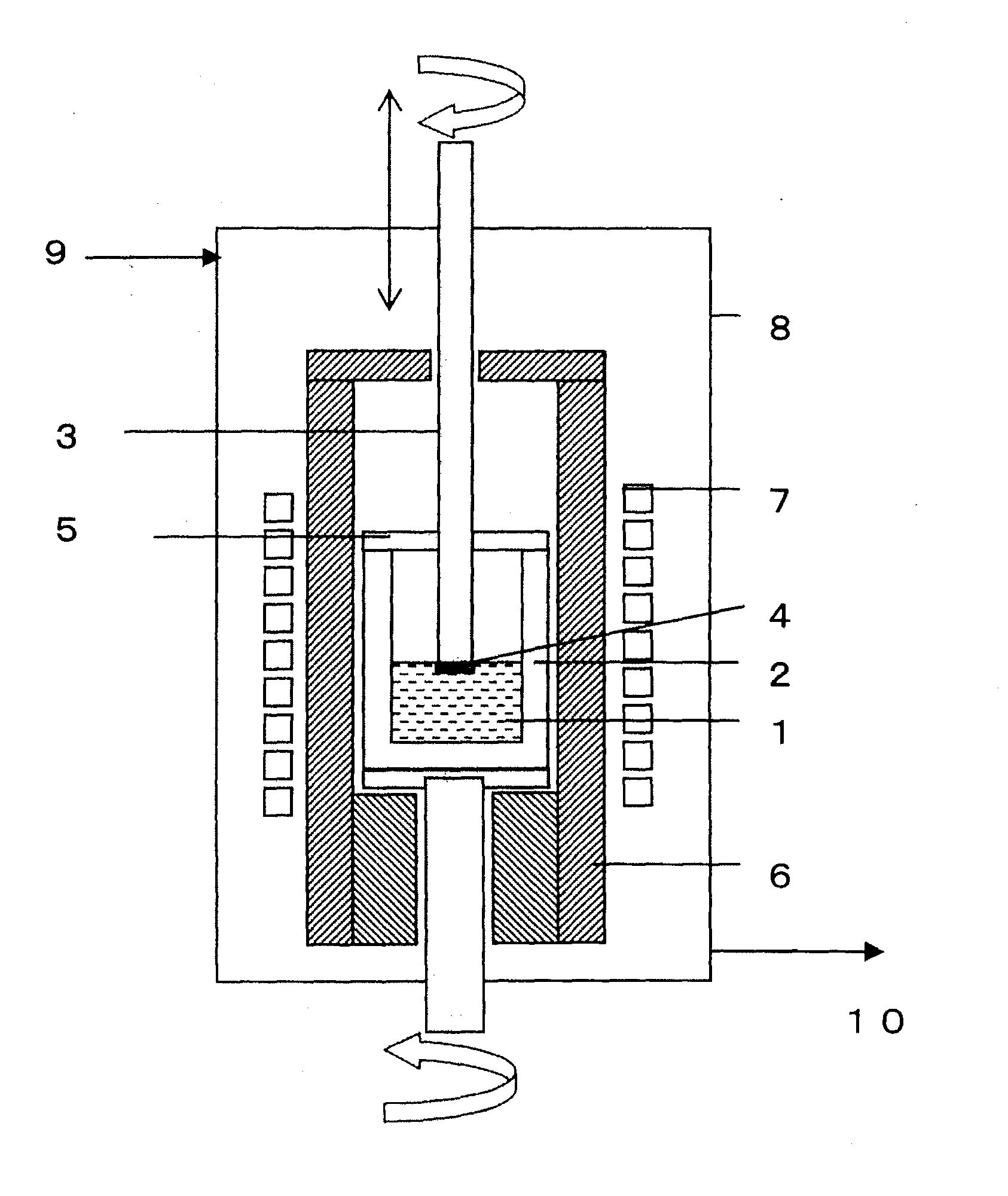
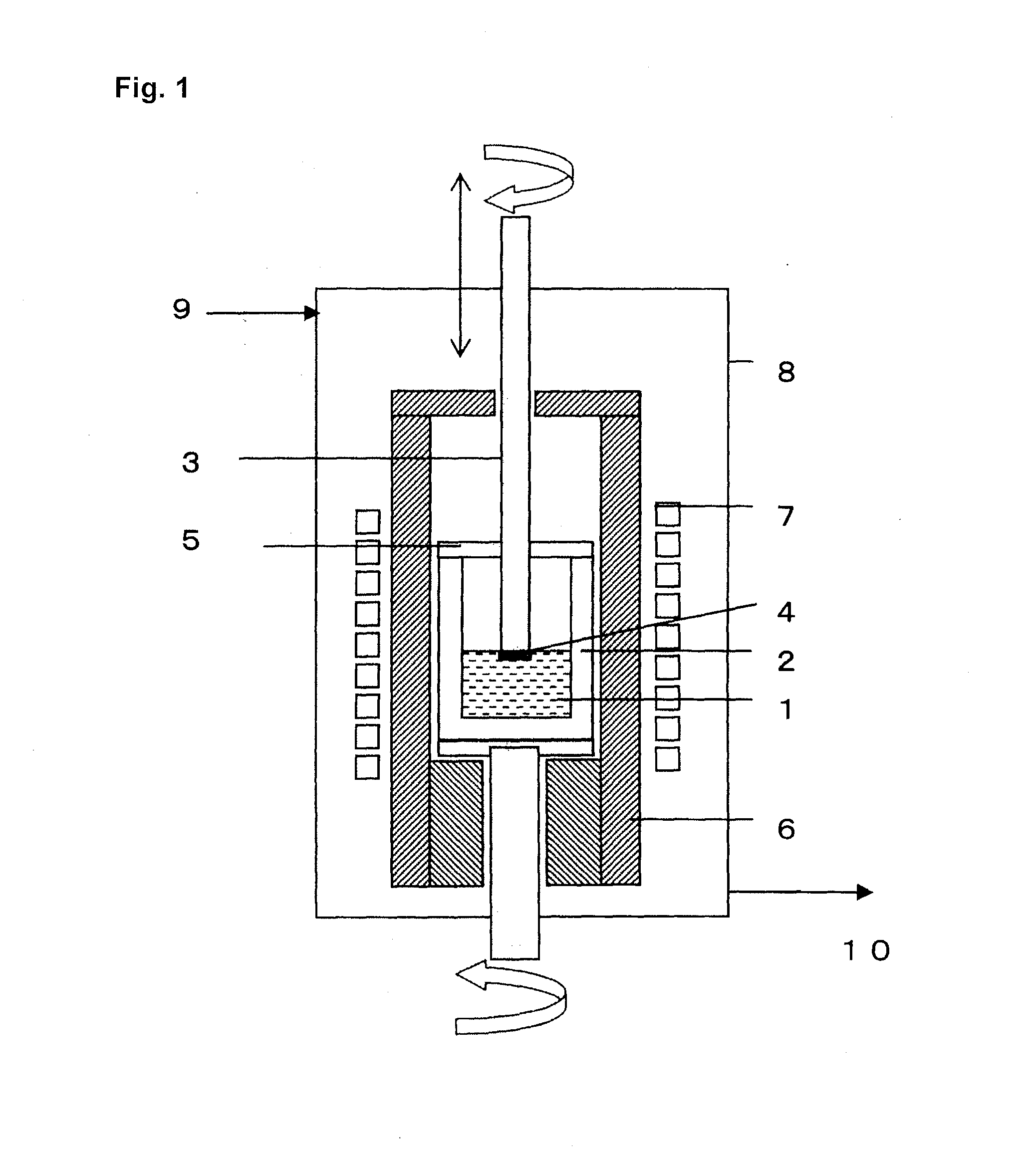
[0056]In this example, an experiment of growth of a SiC single crystal thin film was carried out by the LPE method (temperature gradient method) using the single crystal manufacturing apparatus shown in FIG. 1.

[0057]This single crystal manufacturing apparatus had a crucible 2 of high purity graphite which had an inner diameter of 80 mm and a height of 150 mm and housed therein a SiC solution 1 in the form of a melt. The crucible 2 was disposed in a water-cooled stainless steel chamber 8. The outer periphery of the graphite crucible was surrounded by a heat insulating material 6 for heat retention, and a high frequency coil 7 for inductive heating was disposed around the heat insulating material 6. The temperature distribution in the height direction of the solution could be controlled by adjusting the number of windings of the high frequency coil, the spacing of the windings, and the positional relationship between the graphite crucible and the high frequency coil. The atmosphere wi...


PUM


Abstract

A method capable of stably manufacturing a SiC single crystal in the form of a thin film or a bulk crystal having a low carrier density of at most 5×10¹⁷/cm3 and preferably less than 1×10¹⁷/cm3 and which is suitable for use in various devices by liquid phase growth using a SiC solution in which the solvent is a melt of a Si alloy employs a Si alloy having a composition which is expressed by SixCryTiz wherein x, y, and z (each in atomic percent) satisfy
0.50<x<0.68, 0.08<y<0.35, and 0.08<z<0.35, or  (1)
0.40<x≦0.50, 0.15<y<0.40, and 0.15<z<0.35.  (2)
x, y, and z preferably satisfy 0.53<x<0.65, 0.1<y<0.3, and 0.1<z<0.3.

Description

TECHNICAL FIELD[0001]This invention relates to a method of manufacturing silicon carbide (SiC). A method according to the present invention can be applied to the manufacture of SiC single crystal substrates and SiC epitaxial wafers which are particularly suitable for electronic devices, optical devices, and the like.BACKGROUND ART[0002]Silicon carbide (SiC) has advantageous physical properties such as a wide band gap, a high thermal conductivity, and a low dielectric constant, which make it possible to realize semiconductor devices having a lower operational loss and a high resistance to temperature than silicon (Si) semiconductor devices. As a result, it is expected that silicon carbide can be used in a wide range of applications including as a material for power devices for electric power control, as a material for high frequency devices having high breakdown voltages, as a material for environmentally resistant devices for use in high temperature environments, as a material for r...

Claims


Application Information

Patent Timeline
IPC IPC(8): C30B19/04C30B29/36
CPCC30B9/10C30B19/02C30B29/36C30B19/10C30B19/04H01L21/02
Inventor KAMEI, KAZUHITOKUSUNOKI, KAZUHIKOYASHIRO, NOBUYOSHIYAUCHI, AKIHIROSHIMOSAKI, SHINJI
Owner NIPPON STEEL & SUMITOMO METAL CORP
Why Eureka
Try Eureka