
Method for forming amorphous carbon nitride film, amorphous carbon nitride film, multilayer resist film, method for manufacturing semiconductor device, and storage medium in which control program is stored

a technology of amorphous carbon nitride and amorphous carbon, which is applied in the field of forming amorphous carbon nitride films, multi-layer resist films, and manufacturing semiconductor devices. it can solve the problem of low plasma resistance of arf resists and achieve excellent etching resistance and reduce the reflectance of irradiated light

Inactive Publication Date: 2011-08-18
TOKYO ELECTRON LTD
View PDF22 Cites 10 Cited by
  • Summary
  • Abstract
  • Description
  • Claims
  • Application Information

AI Technical Summary

Benefits of technology

[0008]To address the above problem, the present invention provides an amorphous carbon film formed below a resist film, having excellent etching resistance and capable of reducing reflectance of irradiated light when the resist film is exposed to light.Technical Solution
[0010](1) Etching resistance may be improved as a content of carbon atoms in an amorphous carbon film is increased.
[0013](4) By additionally doping a nitrogen gas into an amorphous carbon film whose content of hydrogen atoms is very low, a possibility that irradiated light is reflected at the amorphous carbon film when a resist film is exposed to light may be decreased.
[0015]Accordingly, an amorphous carbon nitride film having excellent etching resistance and capable of reducing reflectance of irradiated light when a resist film is exposed to light may be formed. Accordingly, the resist film may be accurately patterned when a pattern is formed by using a photolithography technology. Also, a good pattern may be formed on an underlayer film thereof in a following etching process because of high etching resistance, and thus an accurate pattern transfer may be realized without generating deformations in the pattern of an object film to be etched.
[0025]As described above, according to the present invention, an amorphous carbon film having excellent etching resistance and capable of reducing reflectance of irradiated light when a resist film is exposed to light may be formed.

Problems solved by technology

However, the ArF resist has low plasma resistance.

Method used


Image

  • Method for forming amorphous carbon nitride film, amorphous carbon nitride film, multilayer resist film, method for manufacturing semiconductor device, and storage medium in which control program is stored
  • Method for forming amorphous carbon nitride film, amorphous carbon nitride film, multilayer resist film, method for manufacturing semiconductor device, and storage medium in which control program is stored
  • Method for forming amorphous carbon nitride film, amorphous carbon nitride film, multilayer resist film, method for manufacturing semiconductor device, and storage medium in which control program is stored

Examples


Embodiment Construction

[0047]Hereinafter, the present invention will be described in detail by explaining exemplary embodiments of the invention with reference to the attached drawings. Like reference numerals in the drawings and the description below denote like elements, and thus overlapping descriptions will be omitted. Also in the specification, 1 mTorr is (10−3×101325 / 760)Pa and 1 sccm is (10−6 / 60)m3 / sec.

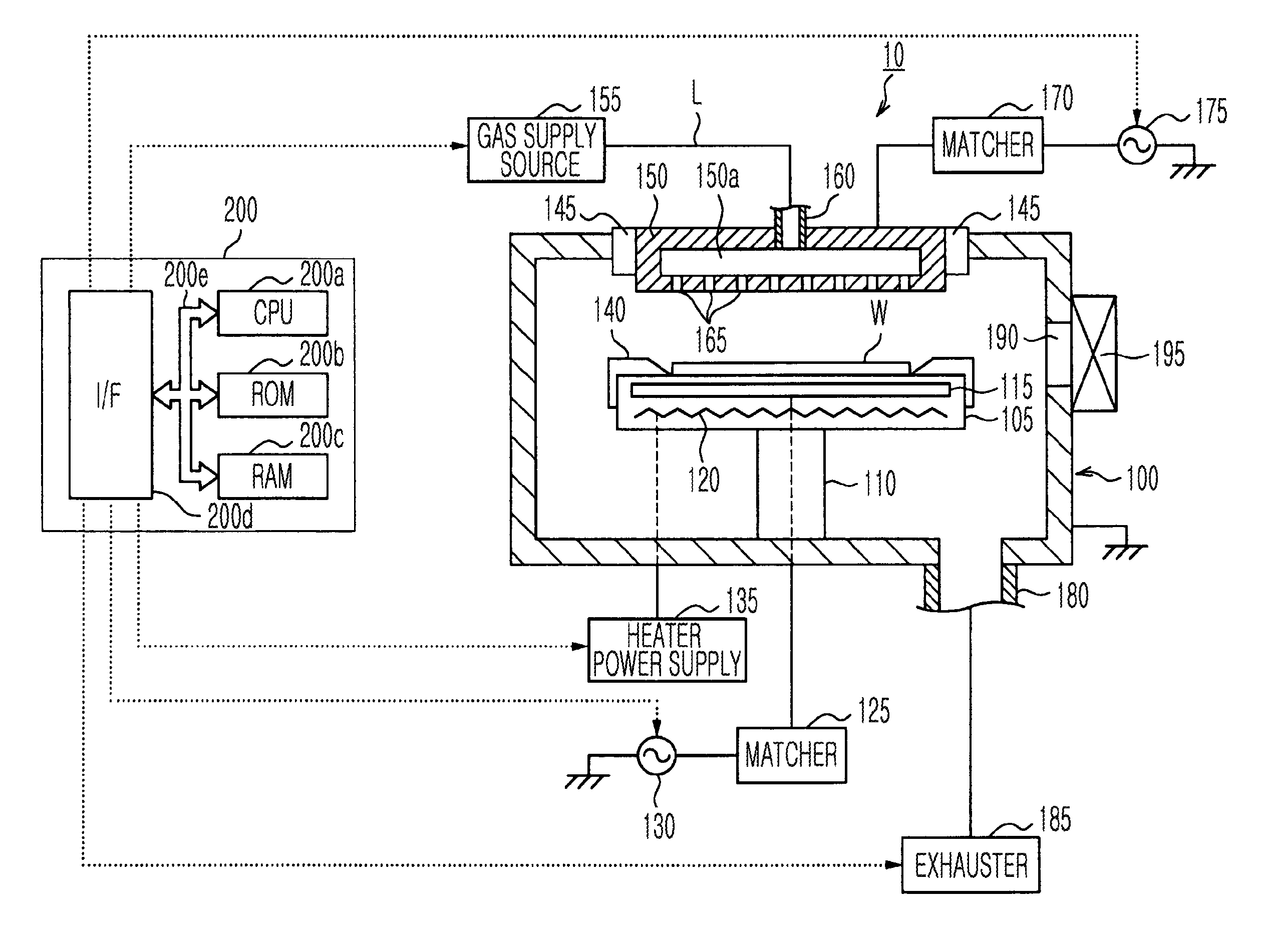
[0048]First, an example of a film-forming process to which a method for forming an amorphous carbon nitride film according to an embodiment of the present invention is applicable will be described by using a plasma CVD apparatus of a parallel plate type. FIG. 1 is a schematic cross-sectional view of a plasma CVD apparatus 10 of a parallel plate type.

[0049](Configuration of Plasma CVD Apparatus)

[0050]The plasma CVD apparatus 10 includes a processing container 100 having a cylindrical shape. The processing container 100 is grounded. A susceptor 105 on which a wafer W is placed is provided inside the pr...


PUM

PropertyMeasurementUnit
wavelengthaaaaaaaaaa
temperatureaaaaaaaaaa

Abstract

An amorphous carbon film, which has excellent etching resistance and is capable of reducing reflectance when a resist film is exposed to light, is form. A method for manufacturing a semiconductor device includes forming an object film to be etched on a wafer, supplying a process gas containing a CO gas and an N2 gas into a processing container, forming an amorphous carbon nitride film from the supplied CO gas and N2 gas, forming a silicon oxide film on the amorphous carbon nitride film, forming an ArF resist film on the silicon oxide film, patterning the ArF resist film, etching the silicon oxide film by using the ArF resist film as a mask, etching the amorphous carbon nitride film by using the silicon oxide film as a mask, and etching the object film to be etched by using the amorphous carbon nitride film as a mask.

Description

TECHNICAL FIELD[0001]The present invention relates to a method for forming an amorphous carbon nitride film applied to a semiconductor device, an amorphous carbon nitride film, a multilayer resist film, a method for manufacturing a semiconductor device, and a storage medium in which a control program is stored.BACKGROUND ART[0002]In manufacturing processes of a semiconductor device, plasma etching is performed by using a photoresist, in which a pattern is formed using a photolithography technology, as an etching mask, and a circuit pattern is transferred to an object film to be etched by the plasma etching. When a pattern is projected onto the photoresist via photolithography, in the CD of a 45 nm generation, an ArF resist is used as the photoresist to achieve minuteness and an ArF laser beam having a wavelength of 193 nm is used as light to which the ArF resist is exposed.[0003]However, the ArF resist has low plasma resistance. Accordingly, a technology of stacking a SiO2 film and ...

Claims


Application Information

Patent Timeline
Patent Type & Authority Applications(United States)
IPC IPC(8): H01L21/311B32B13/04C01C3/00H01L21/31
CPCC23C16/347C23C16/5096G03F7/091H01L21/318H01L21/02274H01L21/31144H01L21/3146H01L21/02115H01L21/0217H01L21/0228C23C16/26H01L21/0274
Inventor ISHIKAWA, HIRAKUNISHIMURA, EIICHI
Owner TOKYO ELECTRON LTD
Learn More