
Inorganic Bulk Multijunction Materials and Processes for Preparing the Same

a multi-junction, inorganic technology, applied in the field of composite materials, can solve the problems of inability to make a significant contribution to the rapidly rising global energy demand, low production cost of silicon-based solar cells, and low economic competitiveness of solar cells with other energy sources

Inactive Publication Date: 2011-09-15
CORNELL UNIVERSITY
View PDF6 Cites 351 Cited by
  • Summary
  • Abstract
  • Description
  • Claims
  • Application Information

AI Technical Summary

Benefits of technology

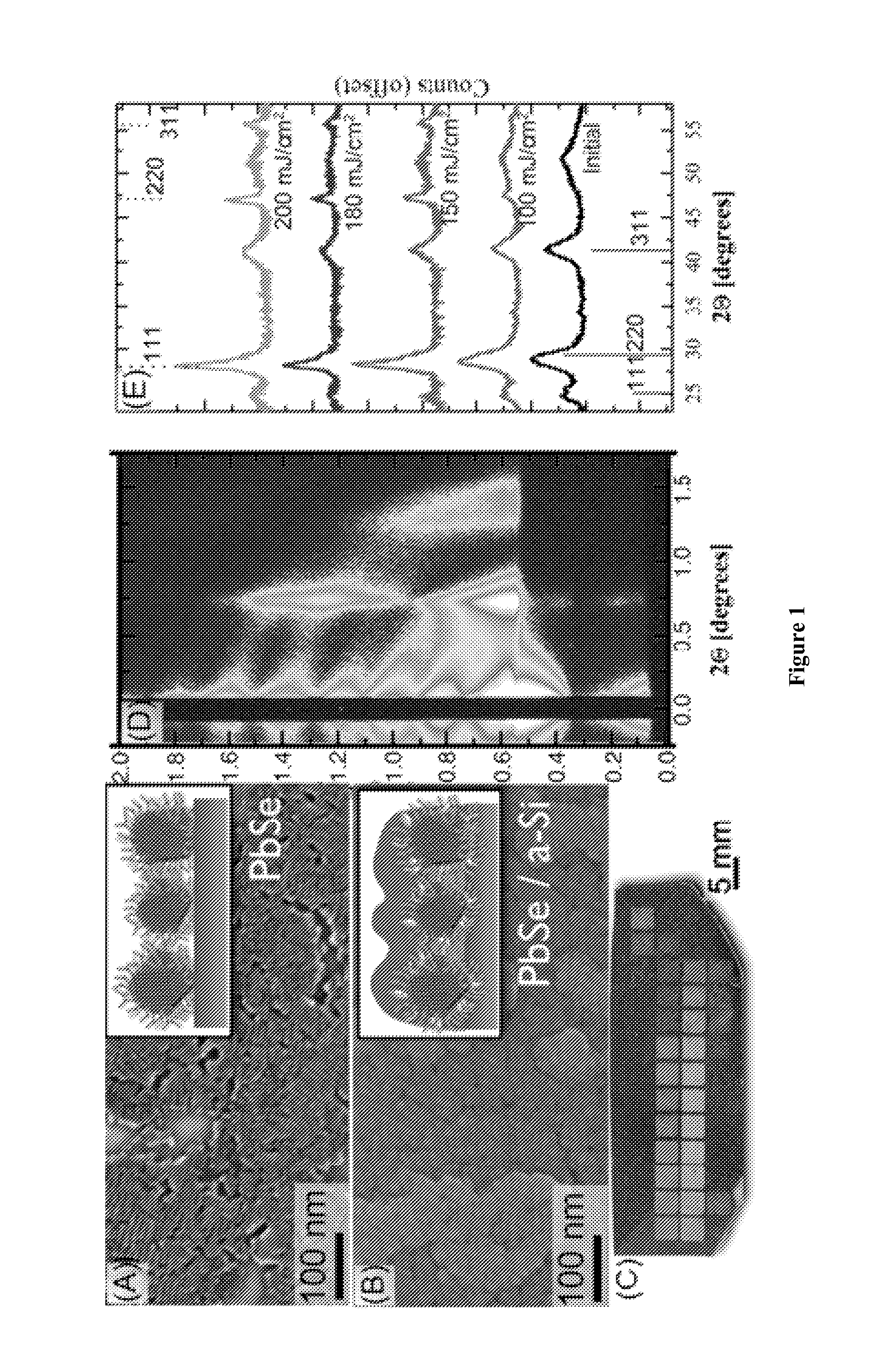
[0009]FIG. 1. SEM images of PbSe NC monolayer before (A) and after (B) sputter deposition of a-Si top layer. (C) Photograph of PbSe / a-Si composite on a Si wafer after exposure to a matrix of laser annealing conditions. (D&E) corresponding small-angle and wide-angle x-ray diffraction of PbSe / polysilicon composites. PbSe (Si) characteristic x-ray diffraction reflections are shown at the bottom (top).

Problems solved by technology

In spite of the vast elemental abundance of silicon and mature and efficient silicon photovoltaic technology, these solar cells are not economically competitive with other energy sources.
The recent steep increase in production volume has steadily dropped the production cost of silicon-based solar cells, however, extrapolation of this trend shows that conventional photovoltaic technology is unable to make a significant contribution to the rapidly rising global energy demands.
The reduced efficiency in polycrystalline silicon solar cells is due to the low mobility of photogenerated carriers, which limits the number of carriers that reach the external electrodes.
Thus, there continues to be an on-going and unmet need for scalable technology to efficiently convert solar and / or thermal energy to electrical energy.

Method used


Image

  • Inorganic Bulk Multijunction Materials and Processes for Preparing the Same
  • Inorganic Bulk Multijunction Materials and Processes for Preparing the Same
  • Inorganic Bulk Multijunction Materials and Processes for Preparing the Same

Examples


example 1

Nanocrystal Synthesis

Colloidal PbSe NCs Will be Synthesized According to a Slightly Modified Version of the Hot-Injection Method

[0080]Thin film processing: The optimal colloidal NCs deposition method depends on a variety of factors. Although spin-casting is the method of choice for most organic thin films, the formation of homogeneous NC films with smooth surfaces and high spatial coherence has favored alternative methods including Langmuir films, drop casting, dip-coating or slow evaporation on tilted substrates. These techniques provide control over a broader range of solvent evaporation rates and are more compatible with additional solution-based processing methods that often accompany NC thin-film processing.

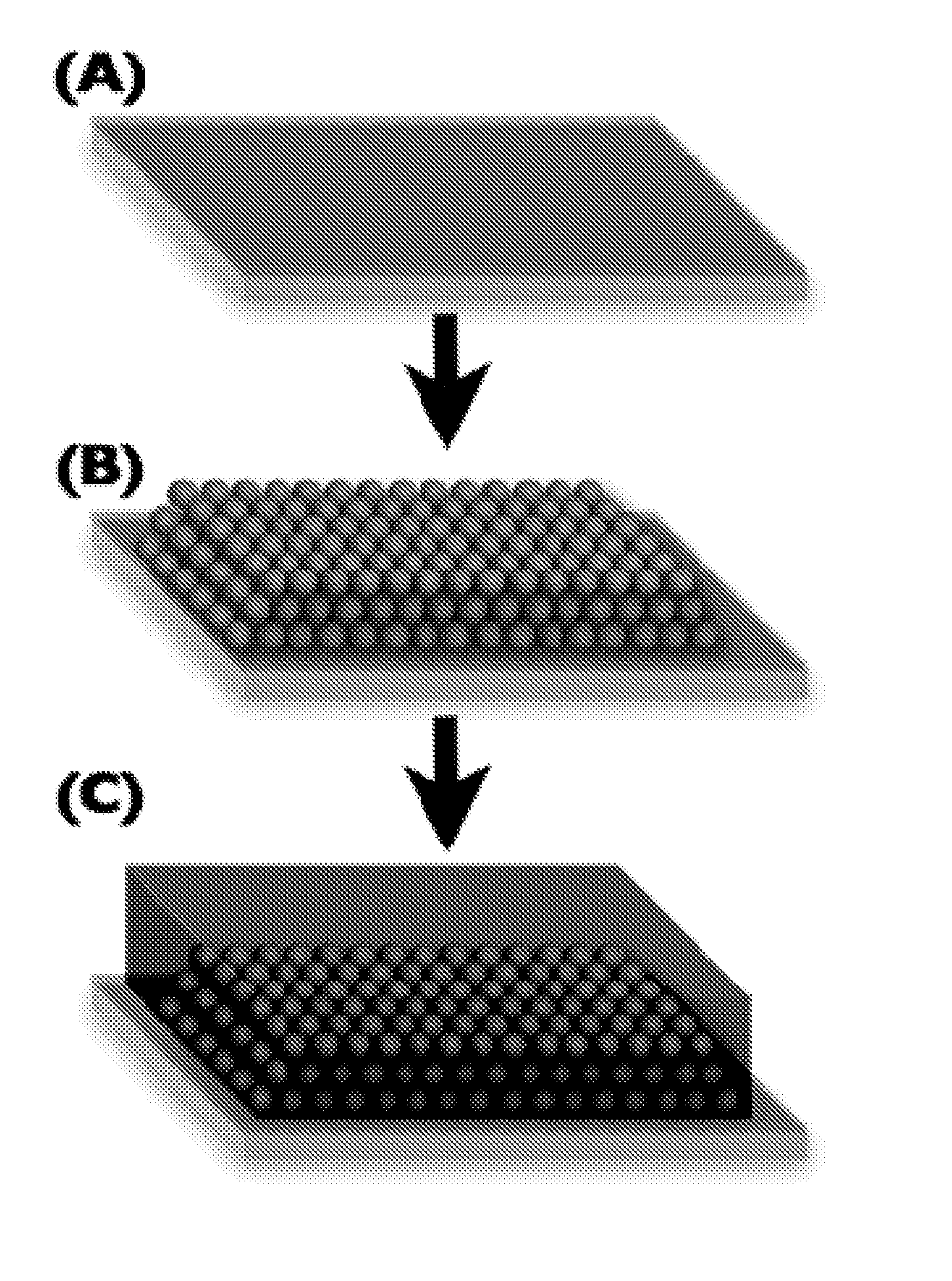
[0081]Two complementary approaches are used to fabricate thin films comprised of PbSe NC encapsulated in an amorphous Si matrix. In the first approach, a NC monolayer is deposited from a colloidal suspension followed by sputter deposition of an amorphous silicon (a-Si) or si...


PUM


Abstract

A nanostructured composite material comprising semiconductor nanocrystals in a crystalline semiconductor matrix. Suitable nanocrystals include silicon, germanium, and silicon-germanium alloys, and lead salts such as PbS, PbSe, and PbTe. Suitable crystalline semiconductor matrix materials include Si and silicon-germanium alloys. A process for making the nanostructured composite materials. Devices comprising nanostructured composite materials.

Description

CROSS-REFERENCE TO RELATED APPLICATIONS[0001]This application claims priority to U.S. Provisional Patent Application No. 61 / 087,455, filed Aug. 8, 2008, which is incorporated herein in its entirety.STATEMENT REGARDING FEDERALLY SPONSORED RESEARCH[0002]This invention was made with government support under grant number CBET 0828703 awarded by the National Science Foundation. The government has certain rights in the invention.FIELD OF THE INVENTION[0003]This invention relates generally to the field of photovoltaic and thermoelectric devices and more particularly to composite materials for use in production of solar cells.BACKGROUND OF THE INVENTION[0004]Over 95% of currently available solar cells are based on silicon. In spite of the vast elemental abundance of silicon and mature and efficient silicon photovoltaic technology, these solar cells are not economically competitive with other energy sources. The recent steep increase in production volume has steadily dropped the production c...

Claims


Application Information

Patent Timeline
IPC IPC(8): H01L29/15H01L21/20
CPCB82Y30/00C01B19/007C01G21/21C01P2002/72C01P2004/03Y02E10/547C01P2004/64H01L31/028H01L31/0312H01L31/035281H01L31/1864C01P2004/04Y02P70/50
Inventor HANRATH, TOBIASENGSTROM, JAMES R.
Owner CORNELL UNIVERSITY
Learn More