Method of testing electronic components

a technology of electronic components and radiation hardness, applied in the field of radiation hardness testing of electronic components, can solve the problems of insufficient testing of a certain electronic component only once, intense, high-energy electrons can be extremely destructive to both man and machine, and the malfunction of electronic devices and circuits

Active Publication Date: 2011-10-06
RADIABEAM TECH
View PDF2 Cites 12 Cited by
  • Summary
  • Abstract
  • Description
  • Claims
  • Application Information

AI Technical Summary

Benefits of technology

[0025]These and other advantages of the invention will become more apparent from the following detailed description thereof and the accompanying exemplary drawings.

Problems solved by technology

This testing has high economic and industrial relevance because electronic components on board of satellites, space vessels, aircraft (“missiles”) and in Earth-based nuclear facilities can be subject to extreme irradiation by different forms of radiation which can lead to malfunction of electronic devices and circuits if they are not adequately designed.
Moreover, it is not enough to test a certain electronic component only once.
These sudden bursts of intense, high-energy electrons can be extremely destructive to both man and machine.
These can be highly dangerous to spacecraft.
Further, other astrophysical objects with magnetic fields such as Jupiter, Saturn etc. also create radiation belt electrons that might pose a danger to spacecraft.
These single events triggered by bombardment of particles can have large detrimental effects and can be highly complex.
Energetic charged particles can activate parasitic transistors, which can then combine into a circuit with a large positive feedback, resulting in a short.
These charges are collected at the source and at the drain, which results in a current pulse emission.
This pulse can be as large as a normal signal applied to the transistor, which results in an unwanted electronic switching operation.
This led to an emergency switch-off, which in turn resulted in an overvoltage spike and an overload, leading to permanent failure.
However, ground-based conventional particle accelerators can not reproduce the exponential electron beam distribution spectrum that occurs in space, and a typical approach to ground-based radiation hardening testing involves investigating the impact of radiation at multiple monochromatic energies, and then extrapolating the results to other energies based on models and assumptions.
These workaround methods are not only inaccurate, but also laborious and expensive, and sometimes inherently cannot capture the physics of specific situations that arise in space.
The primary deficiency in such ground-based approaches is that the naturally occurring space radiation environment energy spectrum (FIG. 2A) is dramatically different from the output of a conventional Earth-bound accelerator (FIG. 2B) because, on Earth, accelerators based on classical technology do not generate particle energy spectra that follow the exponential distribution found to characterize particle energy spectra in space, but instead give nearly monoenergetic distributions.
Considering the energy-dependent stopping powers, it can therefore be concluded that such Earth based electron accelerators are far from well suited to simulate space electron radiation.
Thus, due to increasing miniaturization and computerization, and further due to the increasing number and complexity of space missions, the demand for “beam time” for ground-based component testing is ever increasing despite its shortcomings.
Beam time at test facilities capable of testing such effects in wide parameter ranges is becoming ever more expensive.

Method used


Image

  • Method of testing electronic components
  • Method of testing electronic components
  • Method of testing electronic components

Examples


Embodiment Construction

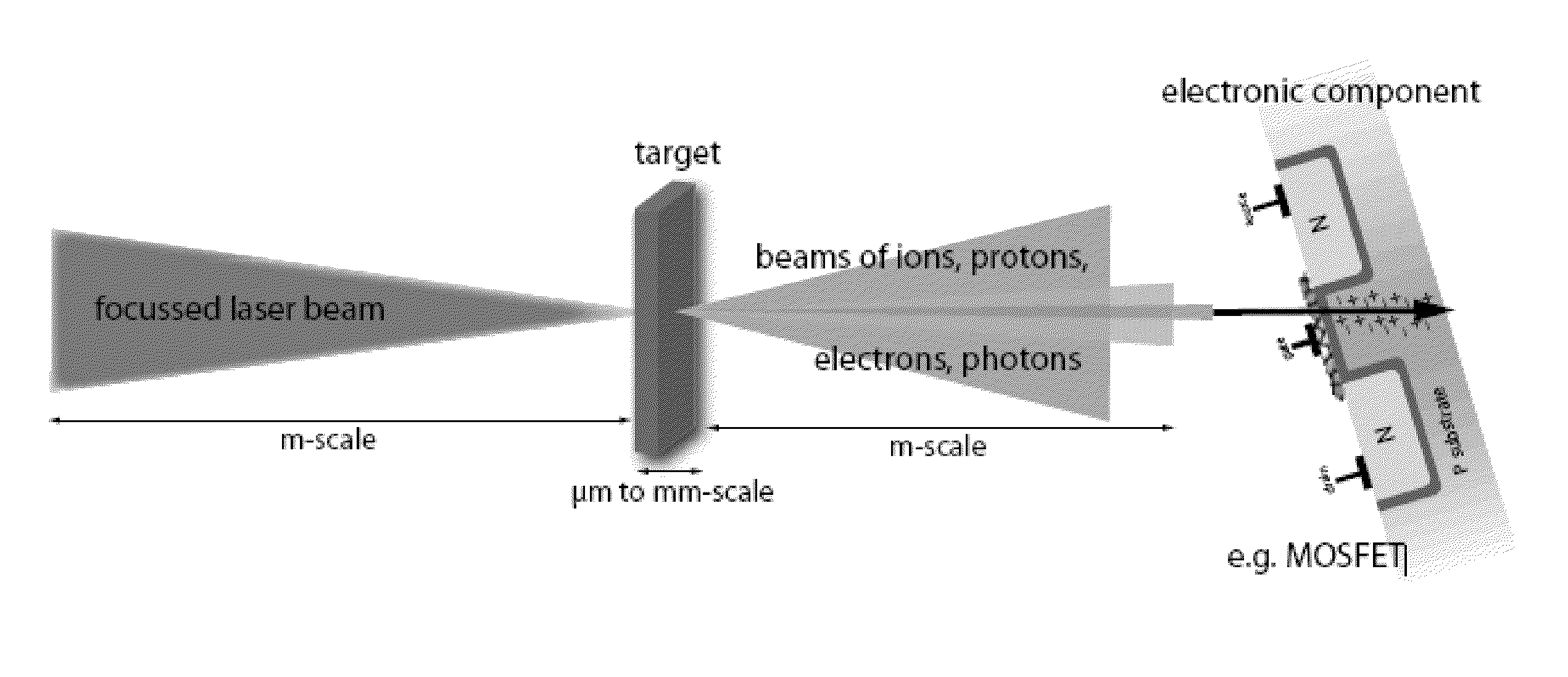
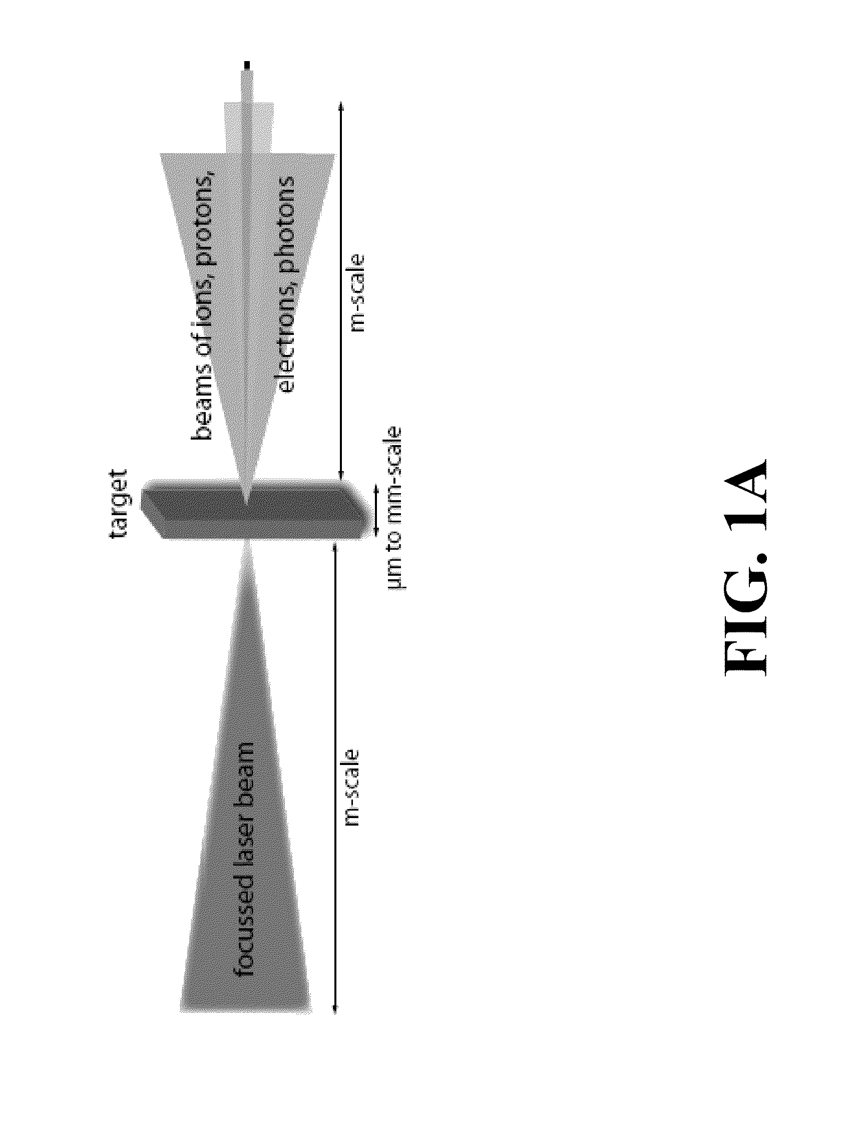
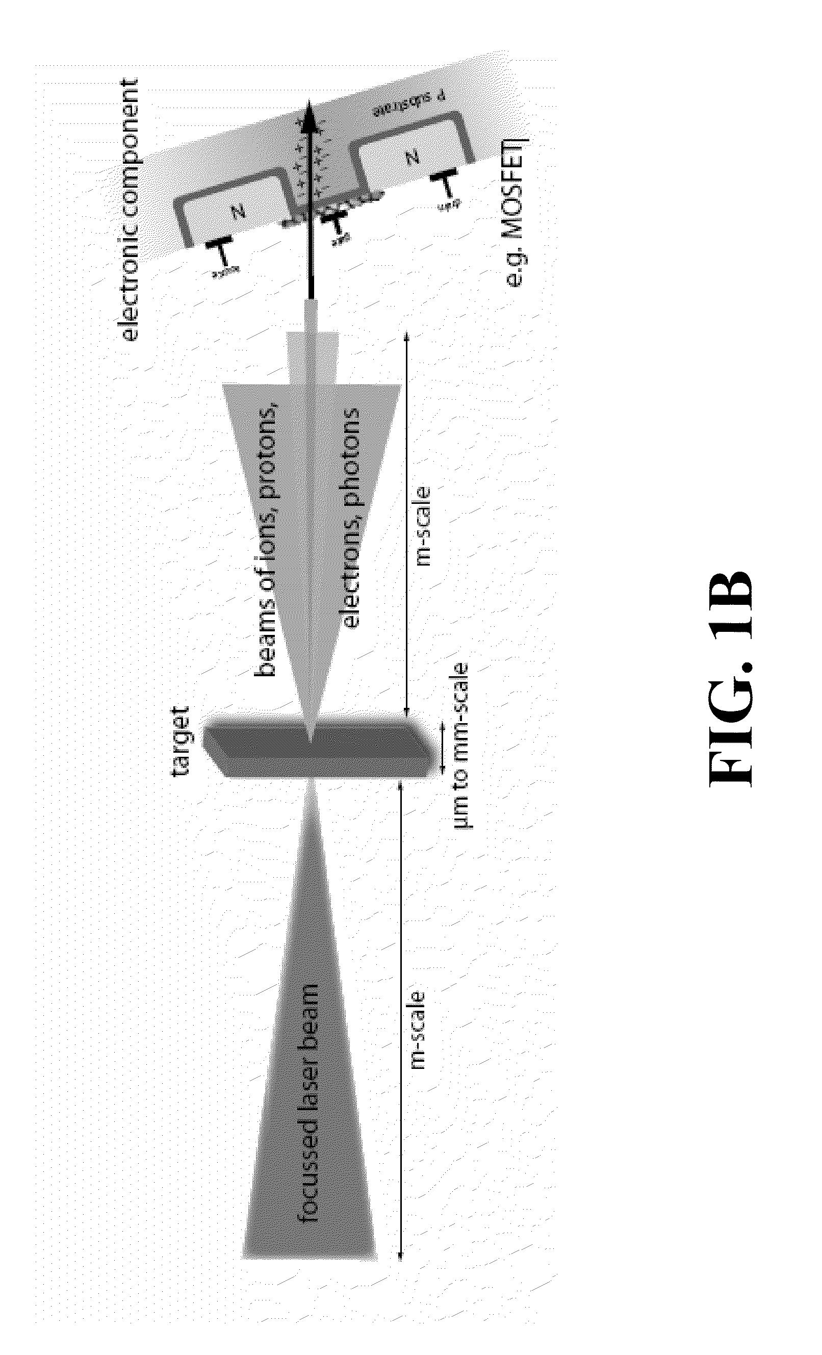
[0041]In conjunction with the Figures, preferred embodiments of the inventive method are described that utilize, under two aspects of the invention described herein, a compact and relatively inexpensive system, a single compact beam of radiation for testing electronic components to ascertain their resistance to various types of high energy radiation encountered in space.

[0042]In a first aspect of the inventive method, the approach of the invention is to utilize a known device that will accelerate particles such as electrons, protons, neutrons, and even ions, based on the interaction of a focused laser beam with matter. This known device is a Laser-Plasma Accelerator (“LPA”), for achieving laser-plasma acceleration. It is known that the LPA is capable of producing, in a single beam, many different types of radiation.

[0043]Yet, to date, this characteristic has not been recognized as providing a useful source of electron energy for the industrial application which is the subject of the...


PUM


Abstract

A method for testing the sensitivity of electronic components and circuits against particle and photon beams using plasma acceleration, in which the flexibility of the multifaceted interaction can produce several types of radiation such as electron, proton, ion, neutron and photon radiation, and combinations of these types of radiation, in a wide range of parameters that are relevant to the use of electronic components in space, such as satellites, at high altitudes or in facilities that work with radioactive substances such as nuclear power plants. Relevant radiation parameter ranges are accessible by this method, which are hardly accessible with conventional accelerator technology. Because of the compactness of the procedure and its versatility, radiation testing can be performed in smaller laboratories at relatively low cost.

Description

BACKGROUND OF THE INVENTION[0001]The present invention relates to a method for testing the radiation hardness of electronic components. This testing has high economic and industrial relevance because electronic components on board of satellites, space vessels, aircraft (“missiles”) and in Earth-based nuclear facilities can be subject to extreme irradiation by different forms of radiation which can lead to malfunction of electronic devices and circuits if they are not adequately designed.[0002]Each spaceship, each probe, each aircraft and, above all, each satellite is packed with electronic components. These components are critically important for the functioning of the missile. For this reason, the resistance of electronic components to be used on board missiles against various types of space radiation is tested extensively prior to launch. Moreover, it is not enough to test a certain electronic component only once. Due to variations found in the quality of different production batc...

Claims


Application Information

Patent Timeline
Patent Type & Authority Applications(United States)
IPC IPC(8): B01J19/12B01J19/08
CPCG01R31/305G01R31/2881
Inventor ROSENZWEIG, JAMESMUROKH, ALEX Y.HIDDING, BERNHARD
Owner RADIABEAM TECH
Why Eureka
Try Eureka