

Method of manufacturing semiconductor device
- Summary
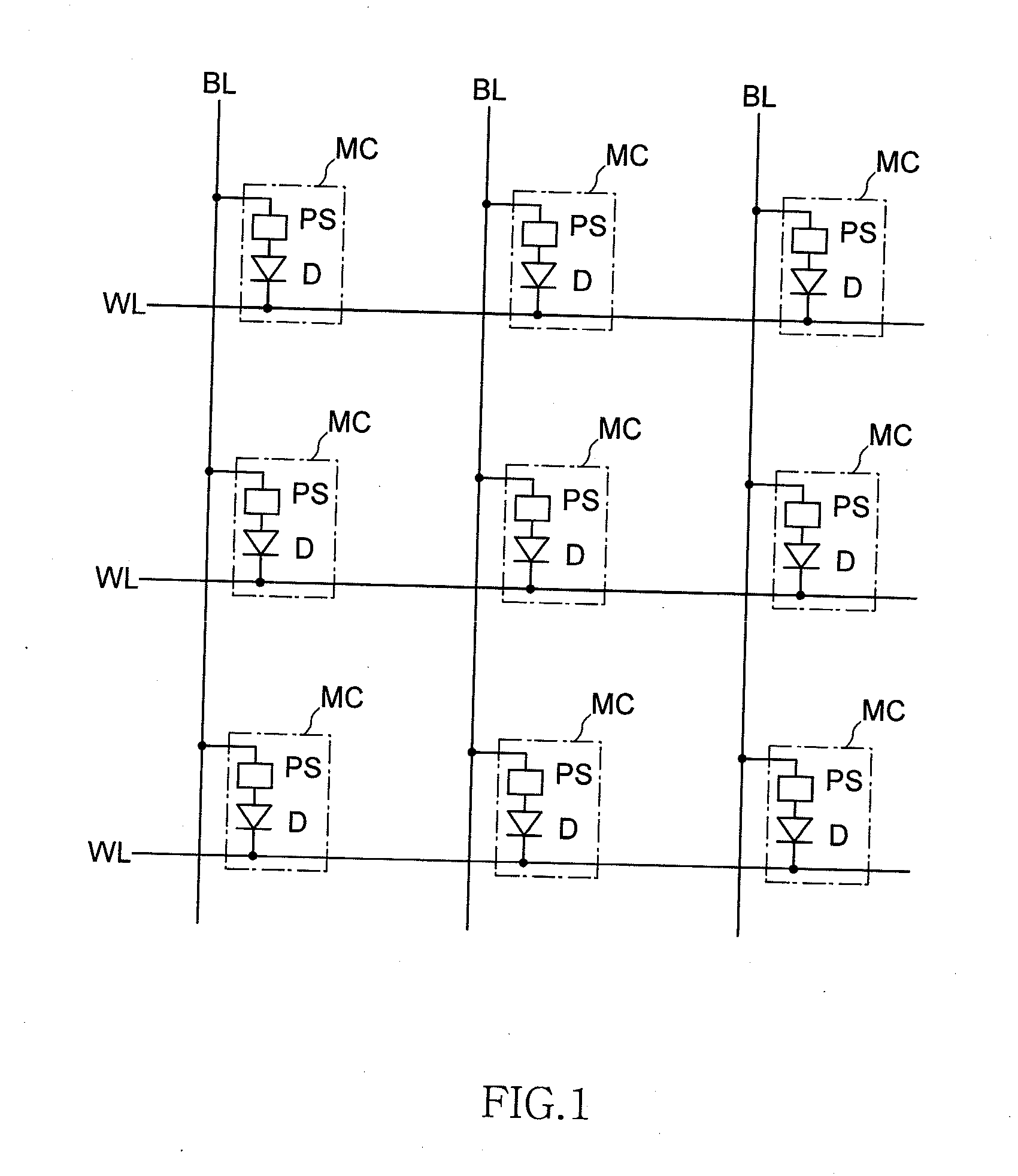
- Abstract
- Description
- Claims
- Application Information
AI Technical Summary
Benefits of technology
Problems solved by technology
Method used
Image

Examples
first embodiment
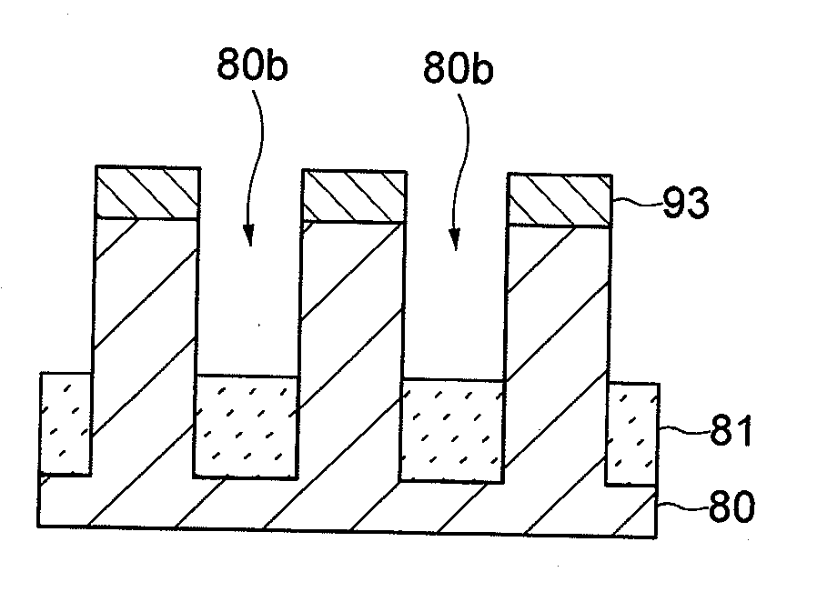
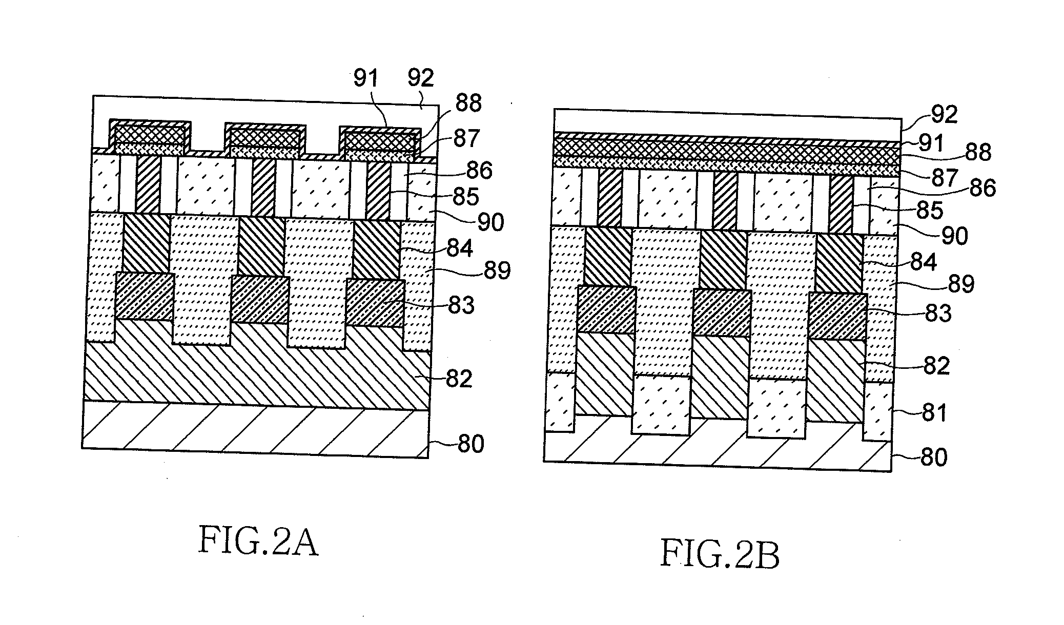
[0036]FIGS. 6A to 19C are diagrams illustrating a process of manufacturing the semiconductor device according to the invention. Hereinafter, a process of forming the upper electrodes 88 will first be described in the process of manufacturing the PRAM exemplified above.
[0037]In the process of manufacturing the semiconductor device according to this embodiment, first, a wiring layer 2, an amorphous carbon film 3, a silicon oxynitride film 4, and a coating film 5 are sequentially formed on a silicon substrate 1, as shown in FIGS. 6A and 6B and FIGS. 7A and 7B. In this embodiment, the silicon substrate 1 is not a non-processed silicon substrate but a substrate which includes respective functional layers such as an impurity diffusion layer, an insulation film, and a metal film.
[0038]The wiring layer 2 is a layer in which the upper electrodes 88 are processed and is formed by sequentially laminating a tungsten film 2a serving as a conductive film and a silicon nitride film 2b serving as a...
second embodiment
[0084]Next, a process of manufacturing a semiconductor device will be described in detail according to the invention.
[0085]In the second embodiment, the organic anti-reflection film which is used as an embedded mask is used even when the peripheral wiring pattern is formed and when a partial cutting pattern of the loop pattern is formed. Since the processes from the process of forming the film in FIGS. 6A and 6B, to the process of forming the silicon oxide film 7 in FIGS. 8A and 8B are the same as those of the first embodiment, the detailed description thereof will not be repeated.
[0086]Next, as shown in FIGS. 36A and 36B and FIGS. 37A to 37C, the two-layered coating film 9 is formed on the entire surface of the substrate. The two-layered coating film 9 includes the organic anti-reflection film 9a and the silicon-containing organic film 9b. The thickness of the organic anti-reflection film 9b is 200 nm and the thickness of the silicon-containing organic film 9b is 30 nm. The organic...
third embodiment
[0098]Next, a process of manufacturing a semiconductor device will be described in detail according to the invention.
[0099]The third embodiment is different from the first and second embodiments in that there is provided dummy spaces 5f at both X-directional ends of the memory cell array region 1A (at areas between an after-mentioned land 5g and line-and-space pattern consisting of the openings 5c and the sidewall cores 5d). As described in detail below, the dummy spaces 5f are provided to prevent the organic anti-reflection film 9a from growing thick on the line-and-space pattern, especially, at areas peripheral to the memory cell array region 1A. Because the finished pattern width tends to change if the thickness of the organic anti-reflection film 9a changes, the dummy spaces 5f can minimize the variety of the pattern width.
[0100]In this embodiment, a case of forming a trench pattern will be described instead of the bit line pattern described in the first and second embodiments. ...
PUM
 Abstract
Description
Claims
Application Information