Physical structure for use in a physical unclonable

a physical structure and physical technology, applied in the field of physical structures for use in physical unclonables, can solve the problems of limited variation of electrical properties and inability to easily control, and achieve the effect of increasing confidence and us

Inactive Publication Date: 2011-10-20
NXP BV
View PDF2 Cites 51 Cited by
  • Summary
  • Abstract
  • Description
  • Claims
  • Application Information

AI Technical Summary

Benefits of technology

[0028]In an embodiment of the method in accordance with the invention the vapor deposition technique used is one of the group comprising: chemical vapor deposition, and atomic layer deposition. The advantage of using these deposition methods is that the surface of the silicon-comprising dielectric layer becomes rough. However, it is not ruled out upfront that other deposition methods will achieve the same result to a higher or to a lesser extent.
[0029]In a third aspect the invention relates to a card or an RFID tag comprising a semiconductor device in accordance with the invention. The card of the invention is preferably a smartcard containing any financial or private data or giving access to any building or information. For such smartcards the safety requirements show a steady increase, which is related to the increasing confidence and use of these smartcards. Alternatively, the card may be a transponder-type of card that can be read out in contactless manner. The card can be a banknote as well. In this case the integrated circuit must be very thin. Another type of a card is a SIM-card for a mobile phone. In case of contactless readout the card will contain an antenna to communicate with the access device. The electronic circuit in the integrated circuit is then connected to said antenna. The physical structure, for example when part of a PUF, can provide for a certain security of the data on the card, as tamper protection and / or data encryption key.

Problems solved by technology

This random component is introduced during the manufacturing process and cannot be easily controlled.
A problem with the known PUF's is that the variation of the respective electrical property is limited.

Method used


Image

  • Physical structure for use in a physical unclonable
  • Physical structure for use in a physical unclonable
  • Physical structure for use in a physical unclonable

Examples


first embodiment

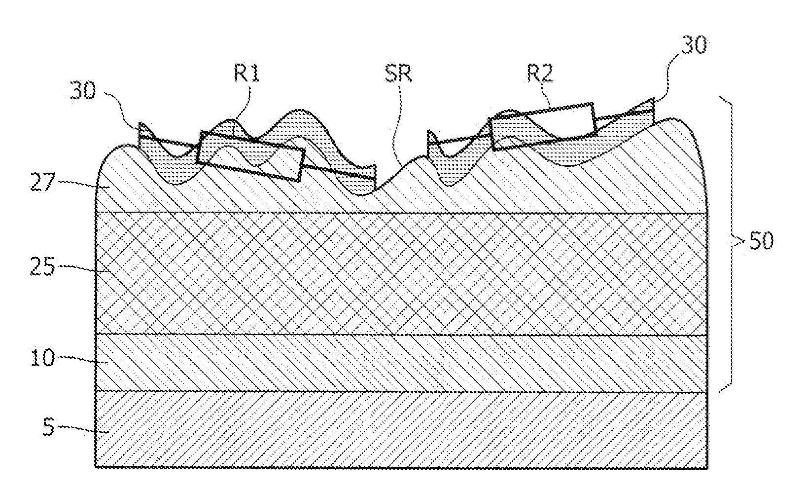
[0042]FIG. 1 shows a cross-sectional view of a semiconductor device with a capacitor for use in a PUF in accordance with the invention. The semiconductor device comprises a substrate 5 comprising a dielectric material, such as silicon oxide at its upper interface in this example. It must be noted that this may be other dielectric materials as well and even conductive materials (i.e. that need to establish a contact with the physical structure). In the substrate 5 there can be electronic components that together form an electronic circuit, such as an FRAM. On the substrate 5 there has been provided an adhesion layer 10, which comprises of a first sub-layer 11 and a second sub-layer 12. The first sub-layer 11 comprises titanium-oxide (TiOx) and the second-sub-layer 12 that has been provided on the first sub-layer 11 comprises titanium (Ti). Further a physical structure 50 is provided on the second sub-layer 12, which in this embodiment comprises a stack of a bottom conductive layer 20...

second embodiment

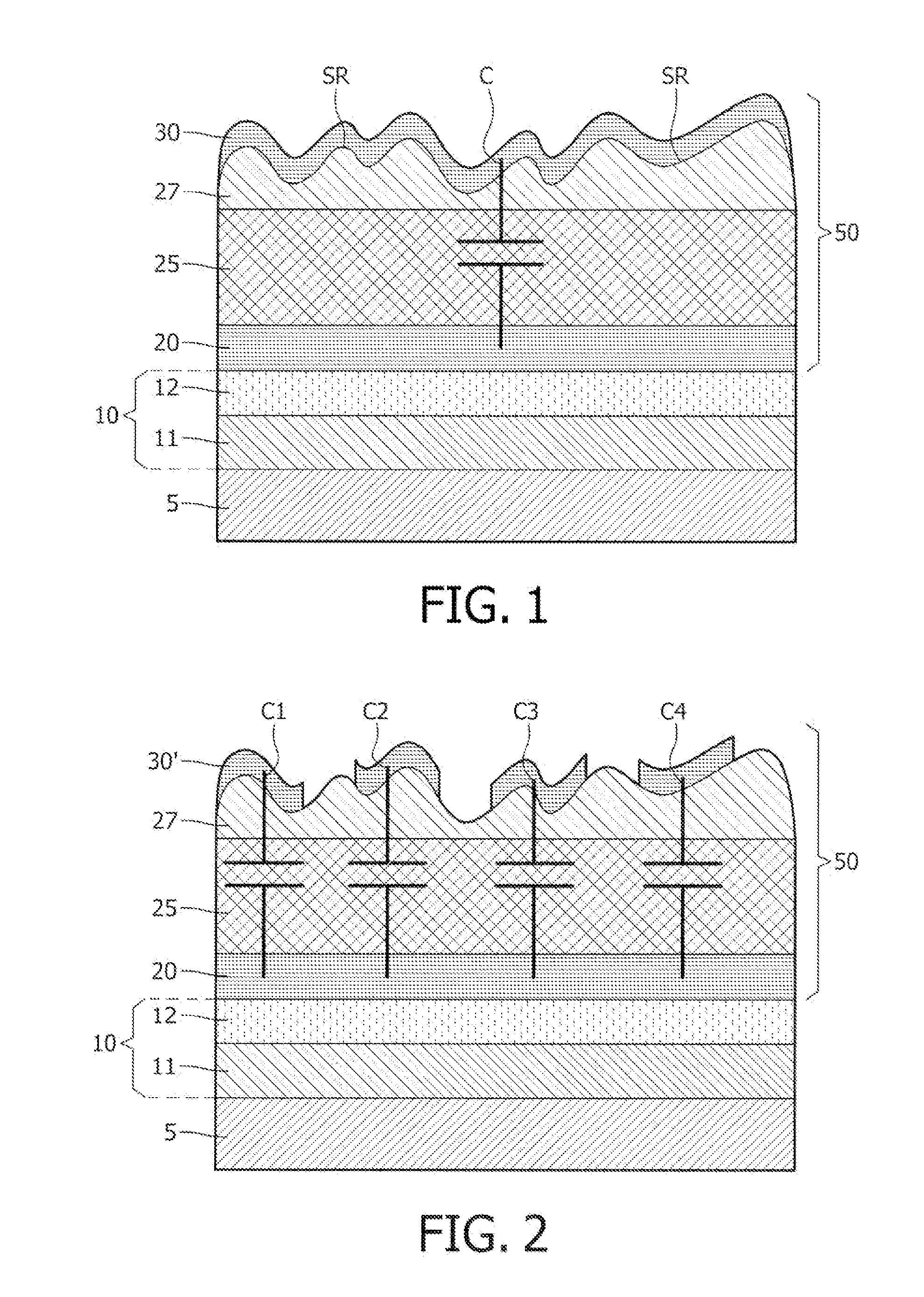
[0050]FIG. 2 shows a cross-sectional view of another semiconductor device with a capacitor for use in a PUF in accordance with the invention. This embodiment will be discussed in as far as it differs from FIG. 1. Whereas in FIG. 1 there is only one capacitor C, in FIG. 2 there is a plurality of capacitors that share a common electrode (the bottom conductive layer). This plurality of capacitors C1, C2, C3, C4 is obtained by patterning the top conductive layer 30′. Depending on the spread in capacitance value of the capacitor in FIG. 1 more or less data bits may be extracted for use in an encryption key in a PUF. In FIG. 2 the plurality of capacitors C1, C2, C3, C4 open up to possibility of extracting even more bits for use in the encryption key. A very important variant of FIG. 2 is a plurality of capacitors C1, C2, C3, C4 wherein the top conductive layer is a common electrode of all capacitors and the bottom conductive layers is patterned so as to form individual electrodes of the p...

third embodiment

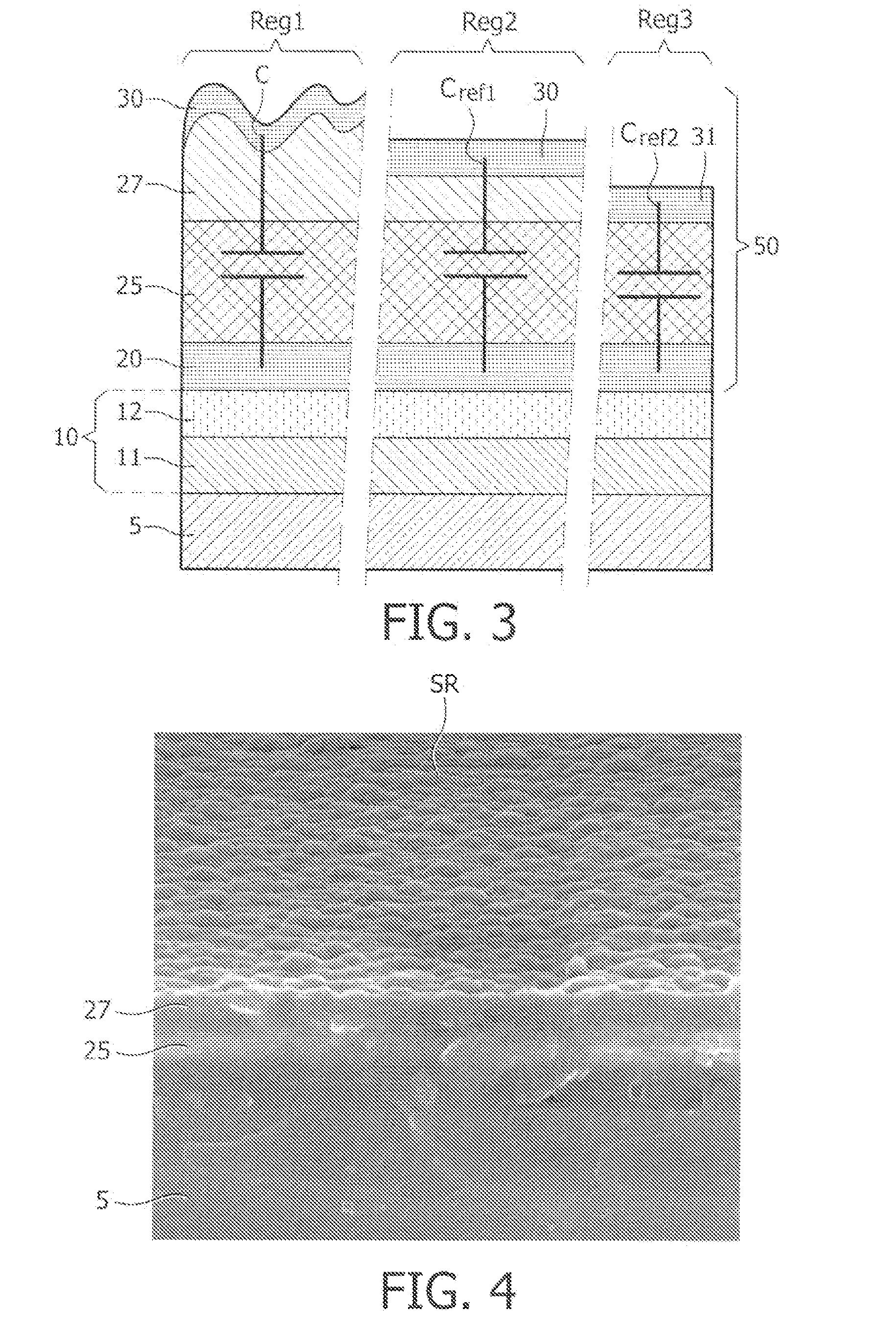
[0051]FIG. 3 shows a cross-sectional view of yet another semiconductor device with a capacitor and two reference capacitors for use in a PUF in accordance with the invention. The semiconductor device has three regions Reg1, Reg2, Reg3. The first region Reg1 comprises the capacitor C as discussed in FIG. 1 or, alternatively, a plurality of capacitors C1, C2, C3, C4 as discussed in FIG. 2. The second region Reg2 comprises a first reference capacitor Cref1. In the first reference capacitor Cref1 the silicon nitride layer 27, onto which the top conductive layer 30 is provided, has no rough surface. The first reference capacitance Cref1 can be manufactured as follows. After manufacturing of the silicon nitride layer 27 a CMP step or anisotropic etch step is carried out which flattens the upper surface of the silicon nitride layer 27. The silicon nitride layer 27 to be formed will then have a flat surface. The resulting reference capacitance Cref1 will have a relatively low k-value betwee...


PUM


Abstract

The invention relates to a semiconductor device comprising a physical structure (50) for use in a physical unclonable function, wherein the physical structure (50) comprises a lead-zirconium titanate layer (25), and a silicon-comprising dielectric layer (27) deposited on the lead-zirconium-titanate layer (25), wherein the silicon-comprising dielectric layer (27) has a rough surface (SR), the physical structure (50) further comprising a conductive layer (30) provided on the rough surface (SR) of the silicon-comprising dielectric layer (27). The invention further relates to a method of manufacturing such semiconductor device. The invention also relates to a card, such as a smartcard, and to a RFID tag comprising such semiconductor device. The inventors have found that depositing of a silicon- comprising dielectric layer (27) on a lead-zirconium titanate layer (25) using vapor deposition results in a silicon-comprising dielectric layer (27) having a rough surface (SR). This rough surface (SR) can be used in a PUF to make a resistor (R) with a variable random value by depositing a conductive layer (30) on the rough surface (SR). Alternatively, the combination of both layers (25, 27) can be used in a PUF as composite dielectric to make a capacitor (C) with a variable random capacitance value.

Description

FIELD OF THE INVENTION[0001]The invention relates to semiconductor device comprising a physical structure for use in a physical unclonable function, to a method of manufacturing such semiconductor device comprising a physical structure for use in a physical unclonable function, and to a card or an RFID tag comprising such semiconductor device.BACKGROUND OF THE INVENTION[0002]Integrated circuits (IC's) for applications such as smartcards, RFID tags, Pay-TV chips often contain a secret security key and carry out secret functions. The IC needs to be secure against attacks from the outside which aim at retrieving data there from. IC's may be subjected to both front-side as well as back-side attacks. In this description the “front-side” of a semiconductor device is defined as the side of the semiconductor device on which circuitry is provided. This side is also being referred to as the “first side of the substrate” in this description. Likewise, the “back-side” of the semiconductor devic...

Claims


Application Information

Patent Timeline
Patent Type & Authority Applications(United States)
IPC IPC(8): H01L29/92H01L21/20
CPCH01L23/576H01L28/55H01L2924/0002H01L2924/00G06F21/73G09C1/00
Inventor ROEST, AARNOUD LAURENSVAN LEUKEN-PETERS, LINDAWOLTERS, ROBERTUS ANDRIANUS MARIA
Owner NXP BV
Why Eureka
Try Eureka