LED display apparatus having active devices and fabrication method thereof

a technology of active devices and display apparatuses, which is applied in the direction of static indicating devices, instruments, solid-state devices, etc., can solve the problems of high voltage and power consumption, large thickness, and heavy weight, and achieve low power consumption, high luminance, and high reliability

Active Publication Date: 2011-11-10
SEOUL NAT UNIV R&DB FOUND
View PDF8 Cites 94 Cited by
  • Summary
  • Abstract
  • Description
  • Claims
  • Application Information

AI Technical Summary

Benefits of technology

[0032]An LED display apparatus of the present invention enables to miniaturize pixel by a formation of wiring on bottom layer and an assembly of each block through each eutectic layer into each transistor block receptor and/or each LED block receptor formed according to each color element unit. Therefore, the LED display apparatus can apply to personal and household applications and can embody AM-LED display apparatus with high luminance, low power consumption, high reliability, and superior optical property by assembling a transistor block having high electron mobility.
[0033]And a fabri

Problems solved by technology

However, the CRT has problems such as a heavy weight, a wide thickness, and a higher voltage and power consumption.
However, the PDP has problems related to low image resolution and high driving voltage.
However, the FED has problems such as a fast thermal degradation of the cathode and a stability of high vacuum state.
However, because the TFT-LCD is one of non-directly emitting elements, it shows bad in the properties of luminance, contrast, sight angle and response speed.
However, the AMOLED has a short life time due to the using an organic electroluminescence diode and is not easy to make a large size due to the difficulty of molding.
Therefore, the passive matrix has some disadvantages such as high power consumption due

Method used


Image

  • LED display apparatus having active devices and fabrication method thereof
  • LED display apparatus having active devices and fabrication method thereof
  • LED display apparatus having active devices and fabrication method thereof

Examples


first embodiment

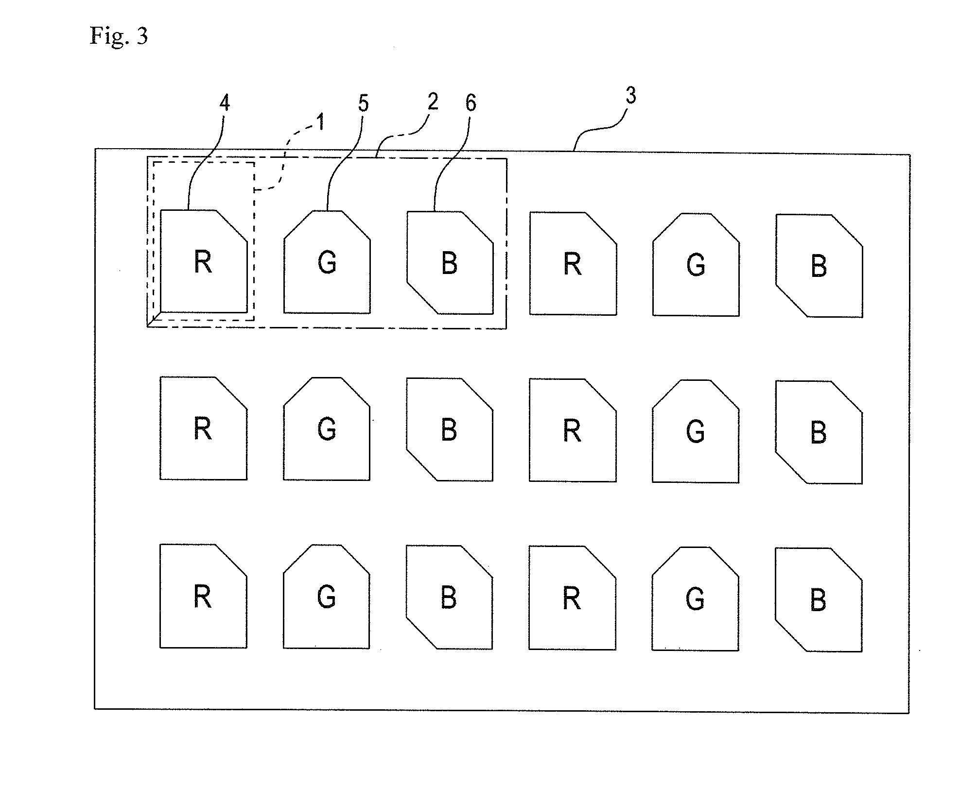
[0065]A structure of an AM-LED display apparatus according to a first embodiment of the present invention comprises basically, as shown in FIG. 3, a plurality of pixels 2 formed on the display substrate 3 and consisted of three color element units 1, respectively. The each color element unit 1 comprises a switching transistor Tr1, a driving transistor Tr2 and an LED. Here, the switching transistor Tr1 and the driving transistor Tr2 are built in the display substrate 3. And the LED is formed by assembling an LED block 4 made previously into a block receptor formed on the substrate 3.

[0066]A plane structure of one color element unit 1 according to the first embodiment is shown with a layout in FIG. 4. The structures formed on the same layer are marked with the same color in FIG. 4.

[0067]As shown in FIGS. 4 to 8, a structure according to the first embodiment is characterized by comprising: a buffer layer 20 formed on a substrate 10; a switching transistor Tr1 active layer (not shown) a...

second embodiment

[0095]A structure of an AM-LED display apparatus according to a second embodiment of the present invention comprises basically, as shown in FIG. 10, a plurality of pixels 2 formed on the display substrate 3 and consisted of three color element units 1, respectively. The each color element unit 1 is formed by assembling a switching transistor block 7, a driving transistor block 8 and an LED block 4 made previously into a switching transistor block receptor, a driving transistor block receptor and an LED block receptor, respectively, which are formed on the substrate 3.

[0096]The plane structure of one color element unit 1 according to the second embodiment is shown with a layout in FIG. 11. The structures formed on the same layer are marked with the same color in FIG. 11.

[0097]As shown in FIGS. 11 to 19, a structure according to the second embodiment is characterized by comprising: a data line 83a, a scan line 80 and a cathode line 60 formed parallel to and separately from each other ...

third embodiment

[0128]A structure of an AM-LED display apparatus according to a third embodiment of the present invention comprises basically, as shown in FIG. 10, a plurality of pixels 2 formed on the display substrate 3 and consisted of three color element units 1, respectively. The each color element unit 1 is formed by assembling a switching transistor block 7, a driving transistor block 8 and an LED block 4 made previously into a switching transistor block receptor, a driving transistor block receptor and an LED block receptor, respectively, which are formed on the substrate 3.

[0129]The plane structure of one color element unit 1 according to the third embodiment is shown with a layout in FIG. 21. The structures formed on the same layer are marked with the same color in FIG. 21.

[0130]As shown in FIGS. 21 to 31, a structure according to the third embodiment is characterized by comprising: a power supply line 82a formed on a substrate 10; a storage capacitor bottom electrode 85a connected electr...


PUM


Abstract

An active matrix LED display apparatus and a fabrication method thereof are provided. The active matrix LED display apparatus enables to miniaturize pixel by a formation of wiring on bottom layer and an assembly of each block through each eutectic layer into each transistor block receptor and/or each LED block receptor formed according to each color element unit, and to be embodied with high luminance, low power consumption, high reliability and superior optical property by assembling a transistor block having high electron mobility. And the fabricating method of the present invention enables to make efficiently an AM-LED display apparatus at room temperature in a short time by using different shapes of receptor and block depending on the function of a transistor and/or on the color of an LED.

Description

CROSS-REFERENCE TO RELATED APPLICATION[0001]This application claims priority under 35 U.S.C. 119 of Korean Patent Application 10-2010-0042869 filed on May 7, 2010, the entire contents of which are hereby incorporated by reference.BACKGROUND OF THE INVENTION[0002]1. Field of the Invention[0003]The present invention relates to an active matrix display apparatus and a method for fabricating the same, and more particularly, to an active matrix LED display apparatus having an active matrix consisting of a transistor and a light emitting diode (LED) and to a fabrication method thereof.[0004]2. Description of the Related Art[0005]So far, the display devices are known such as a cathode ray tube (CRT), a plasma display panel (PDP), a field emission display (FED), a thin film transistor-liquid crystal display (TFT-LCD), and an active-matrix organic light-emitting diode (AMOLED).[0006]The advantages and disadvantages of the known display devices are as like as followings.[0007]The CRT is used ...

Claims


Application Information

Patent Timeline
IPC IPC(8): G09G3/32H01L33/62G06F3/038
CPCH01L25/167H01L27/1214H01L27/1255H01L33/20H01L33/40H01L2924/12041H01L24/95H01L2224/95085H01L2924/00H01L2924/01322H01L2924/12044H01L2924/12036
Inventor PARK, BYUNG GOOKSEO, CHANG SUYOO, BYUNG DOOHONG, KEUN KEEJEE, SANG YEOPJEONG, JAE MIN
Owner SEOUL NAT UNIV R&DB FOUND
Why Eureka
Try Eureka