Supercharge Your Innovation With Domain-Expert AI Agents!

Dram cell utilizing floating body effect and manufacturing method thereof

a floating body effect and memory cell technology, applied in the field of memory cells and manufacturing methods thereof, can solve the problems of not being compatible with the conventional cmos ulsi manufacturing process, complicated manufacturing process, and difficulty in scaling down the feature size of conventional embedded dram (edram), so as to reduce the area of memory and improve the integration density

Active Publication Date: 2011-12-01
SHANGHAI INST OF MICROSYSTEM & INFORMATION TECH CHINESE ACAD OF SCI
View PDF3 Cites 11 Cited by
  • Summary
  • Abstract
  • Description
  • Claims
  • Application Information

AI Technical Summary

Benefits of technology

The present invention provides a DRAM cell and a manufacturing method using isolated floating body on SOI or GOI as a storage node, which reduces the area of the memory and improves integration density. The DRAM cell includes a buried oxide layer, a first P type semiconductor region, a N type semiconductor region, and a second P type semiconductor region. An electrical isolation region is formed around the N type semiconductor region to isolate it from other cells. A depletion region is formed by the first and second P type semiconductor regions. A bit line electrode is provided on the second P type semiconductor region. The method of manufacturing the DRAM cell includes steps of preparing a substrate, preparing a shallow trench isolation region, preparing semiconductor regions, preparing a gate dielectric material, and preparing a gate electrode material. The DRAM cell has a reduced area and improved integration density.

Problems solved by technology

The conventional embedded DRAM (eDRAM) is facing more and more difficulties in scaling down the feature size.
It is very complicated to prepare stack capacitor by adopting high k material or prepare trench capacitor of high aspect ratio during the IC manufacturing process.
Therefore the manufacturing process is very complicated and is not compatible with conventional CMOS ULSI manufacturing process.
Therefore, the application of the eDRAM to SoC is limited.
The drawback of this memory cell is that the circuit and logic design is complicated and the leakage current is hardly controlled.

Method used


Image

  • Dram cell utilizing floating body effect and manufacturing method thereof
  • Dram cell utilizing floating body effect and manufacturing method thereof
  • Dram cell utilizing floating body effect and manufacturing method thereof

Examples


Embodiment Construction

[0060]The present invention is further explained in detail according to the accompanying drawings. It should be noted that figures are schematic representations of devices, and not drawn to scale.

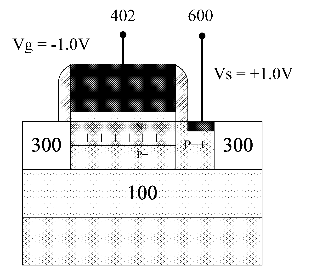
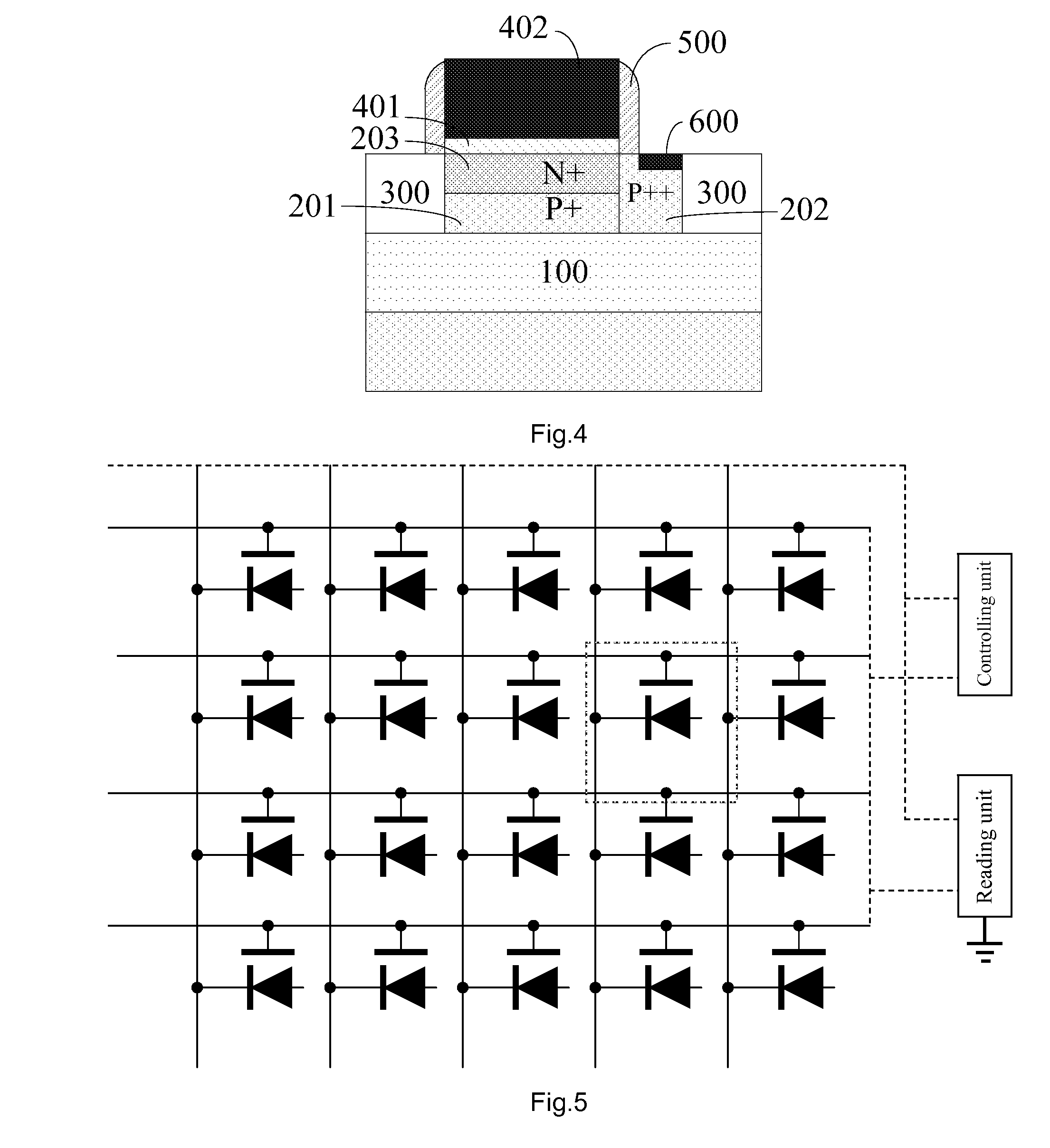
[0061]Referring to FIG. 4 of the drawings, a high efficient DRAM cell utilizing floating body effect based on the tunneling effect between bands comprises a buried oxide layer (BOX) 100, a first P type semiconductor region 201 provided on the buried oxide layer 100, a N type semiconductor region 203 provided on the first P type semiconductor region 201, a gate region provided on the N type semiconductor region 203, a second P type semiconductor region 202 provided on one side of the N type semiconductor region 203, wherein the second P type semiconductor region 202 communicates with the first P type semiconductor region 201, wherein the N type semiconductor region 203, the second P type semiconductor region 202 and the first P type semiconductor region 201 forms an active region, and a shal...


PUM


Abstract

The present invention discloses a DRAM cell utilizing floating body effect and a manufacturing method thereof. The DRAM cell includes a P type semiconductor region provided on a buried oxide layer, an N type semiconductor region provided on the P type semiconductor region, a gate region provided on the N type semiconductor region, and an electrical isolation region surrounding the P type semiconductor region and the N type semiconductor region. A diode of floating body effect is taken as a storage node. Via a tunneling effect between bands, electrons gather in the floating body, which is defined as a first storage state; via forward bias of PN junction, electrons are emitted out from the floating body or holes are injected into the floating body, which is defined as a second storage state. The present invention provides a highly efficient DRAM cell utilizing floating body effect with high density, which has low power consumption, has simple manufacturing process, and is compatible to the conventional CMOS and conventional logic circuit manufacturing process.

Description

BACKGROUND OF THE PRESENT INVENTION[0001]1. Field of Invention[0002]The present invention relates to a memory cell and a manufacturing method thereof, and particularly to a DRAM (dynamic random access memory) cell utilizing floating body effect (FBE) and a manufacturing method thereof, which belongs to semiconductor manufacturing field.[0003]2. Description of Related Arts[0004]With development of the ULSI (Ultra Large Scale Integration), processing unit, memory cell, analog circuit, logical interface, and even RF circuit are integrated into a single chip, forming a so called SoC (System on Chip). As important parts of SoC, embedded memory and logic circuit are integrated into a single chip, which takes more than 50% of the microprocessor or system chip area, and may take more area according the application requirement. The feature size of CMOS will continue to scale down to less than 40 nm according to Moore's law. The conventional embedded DRAM (eDRAM) is facing more and more diffi...

Claims


Application Information

Patent Timeline
Patent Type & Authority Applications(United States)
IPC IPC(8): G11C11/38H01L21/336H01L29/772H10B12/00
CPCG11C11/404H01L29/7841H01L27/10802G11C2211/4016H10B12/20
Inventor XIAO, DEYUANHUANG, XIAOLUCHEN, JINGWANG, XI
Owner SHANGHAI INST OF MICROSYSTEM & INFORMATION TECH CHINESE ACAD OF SCI
Features
  • R&D
  • Intellectual Property
  • Life Sciences
  • Materials
  • Tech Scout
  • Unparalleled Data Quality
  • Higher Quality Content
  • 60% Fewer Hallucinations
Learn More