Check patentability & draft patents in minutes with Patsnap Eureka AI!

NAND-BASED 2T2b NOR FLASH ARRAY WITH A DIODE CONNECTION TO CELL'S SOURCE NODE FOR SIZE REDUCTION USING THE LEAST NUMBER OF METAL LAYERS

a cell array and diode connection technology, applied in the field of cell array architecture of nonvolatile nand-based nor flash memory devices, can solve the problems of inability to make the channel length the channel length cannot be made with the smallest feature size in the most advanced process, and the scalability becomes worse, so as to achieve the effect of symmetrical memory cell high scalability, less tunneling oxide degradation, and smallest featur

Inactive Publication Date: 2011-12-01
APLUS FLASH TECH
View PDF2 Cites 15 Cited by
  • Summary
  • Abstract
  • Description
  • Claims
  • Application Information

AI Technical Summary

Benefits of technology

"The present invention provides a novel memory array architecture and operation for a nonvolatile two transistor two bit (2T2b) NAND-based fast-random-read NOR flash cell. The invention solves the drawbacks of conventional NOR flash memories and provides a unified combo NAND and NOR flash design for both code and data storages in mobile handset applications. The invention also provides a smallest feature size in advanced technology, uses FN channel program and FN channel erase schemes for the flash memory, applies an appropriate voltage to the source line, and provides a Schottky diode between the source line and the memory cell. The invention also provides a pillar-structured polysilicon diode, a P / N+ silicon diode, and a P / N+ silicon diode between the source line and the source node of the memory cell. The technical effects of the invention include improved performance, reduced tunneling oxide degradation, and high P / E endurance cycles."

Problems solved by technology

In other words, the scalability becomes worse when the advanced technology has a small geometry such as 130 nm or below.
However, the requirement of two source line (SL) and bit line (BL) select gate transistors along the NAND string to isolate from other NAND string requires certain extra percentage of overhead in the size of the whole memory array.
Due to the punch-through concern on those two SL and BL select gate transistors, their channel length can not be made with the smallest feature size in the most advanced process either.
In other words, the smallest feature size can only be applied to the memory cell with the cost of more percentage of overhead for the SL and BL select gate transistors.
However, the problem of punch-through effect is just moved from the memory cell to the access transistor.
This causes a physical limitation on how small the cell can be made and in turn limits the use of the cell in ultra high integrated levels of the flash memory below 0.18 μm technology.
Furthermore, the negative FN-edge programming causes device oxide degradation because the electron-hole pairs at the biased drain / TPW (triple P-Well) junction are accelerated by the voltage difference between the drain and source nodes.
However, the drain induced leakage current may occur if the channel length is scaled down.
Therefore, the flash cell still faces the scaling issue and can only be manufactured with a large memory cell size.
In the memory array, the same scaling issue exists.

Method used


Image

  • NAND-BASED 2T2b NOR FLASH ARRAY WITH A DIODE CONNECTION TO CELL'S  SOURCE  NODE  FOR  SIZE REDUCTION  USING THE LEAST NUMBER OF METAL LAYERS
  • NAND-BASED 2T2b NOR FLASH ARRAY WITH A DIODE CONNECTION TO CELL'S  SOURCE  NODE  FOR  SIZE REDUCTION  USING THE LEAST NUMBER OF METAL LAYERS
  • NAND-BASED 2T2b NOR FLASH ARRAY WITH A DIODE CONNECTION TO CELL'S  SOURCE  NODE  FOR  SIZE REDUCTION  USING THE LEAST NUMBER OF METAL LAYERS

Examples


Embodiment Construction

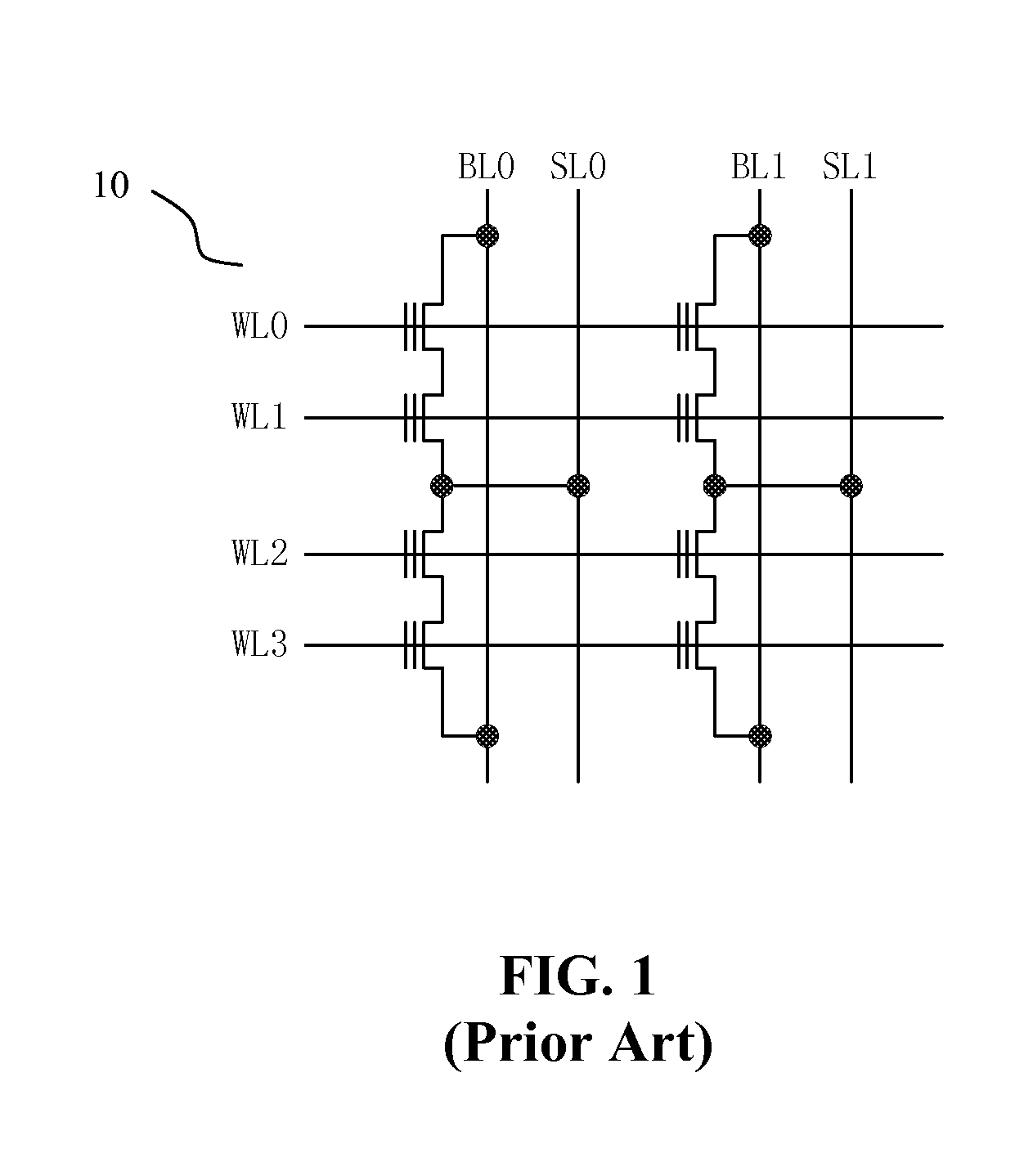
[0055]FIG. 3A is a schematic diagram 30 of a 1T NOR flash memory array of the present invention in which a diode is used to connect the source node of each individual memory cell to one common source line. The memory array is composed of bit lines BL0-BL1, word lines WL0-WL1 and one common source line SL. By connecting the source line at the positive end of the diode, the source node of each memory cell is connected to the negative end of the diode.

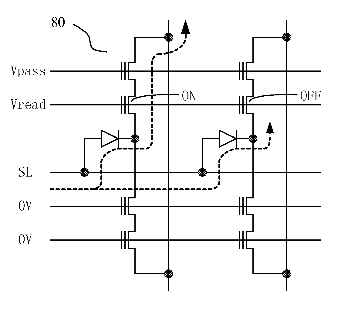
[0056]FIG. 3B is a schematic diagram 40 of a modified 2T string NAND-based NOR flash memory array of the present invention by using a diode to connect the source node of each individual memory cell to one common source line. This memory array is composed of bit lines BL0-BL1, word lines WL0-WL3 and one common source line SL. By connecting the source line at the positive end of the diode, the source node of each memory cell is connected to the negative end of the diode.

[0057]FIG. 3C is a schematic diagram 50 of a modified NT string NAND fl...


PUM


Abstract

A NAND-based NOR flash memory array has a matrix of NAND-based NOR flash cells arranged in rows and columns. Every two adjacent NAND-based NOR flash cells in a column share a common source node which is connected to a common source line through a diode. The source line may be made of a metal layer and is in contact directly with the source node or through an ohmic contact to form a Schottky barrier diode. The source line may also be made of a polysilicon or metal layer and connected to the source node through a pillar-structured polysilicon diode and a conduction layer. The diode may also be formed in the source node by enclosing a P / N+ junction diode in a heavily N+ doped region of the source node.

Description

CROSS-REFERENCE TO RELATED APPLICATIONS[0001]This application claims priority under 35 U.S.C. §119 to U.S. Provisional Patent Application Ser. No. 61 / 396,553, filed on May 28, 2010, assigned to the same assignee as the present invention, and incorporated herein by reference in its entirety.BACKGROUND OF THE INVENTION[0002]1. Field of the Invention[0003]The present invention relates generally to the cell array architecture of nonvolatile memory devices, and more particularly to the cell array architecture of nonvolatile NAND-based NOR flash memory devices.[0004]2. Description of Related Art[0005]Nonvolatile memory is well known in the art. The different types of nonvolatile memory include read-only-memory (ROM), electrically programmable read only Memory (EPROM), electrically erasable programmable read only memory (EEPROM), NOR flash memory, and NAND flash memory. In current applications such as personal digital assistants, cellular telephones, notebook and laptop computers, voice re...

Claims


Application Information

Patent Timeline
Patent Type & Authority Applications(United States)
IPC IPC(8): G11C16/10G11C16/16
CPCG11C16/0433G11C16/0483H01L29/872H01L27/11524H01L27/1021H10B41/35
Inventor HSU, FU-CHANGLEE, PETER WUNG
Owner APLUS FLASH TECH
Features
  • R&D
  • Intellectual Property
  • Life Sciences
  • Materials
  • Tech Scout
  • Unparalleled Data Quality
  • Higher Quality Content
  • 60% Fewer Hallucinations
Learn More