Miniaturized piezoelectric accelerometers

a piezoelectric accelerometer and micro-cantilever technology, applied in the direction of speed/acceleration/shock measurement, measurement devices, instruments, etc., can solve the problems of reducing the magnitude of the electrical voltage output of the miniaturized, and affecting the accuracy of the measurement. achieve the effect of improving structural robustness and flexibility, high miniaturization size, and enhancing sensitivity

Active Publication Date: 2011-12-08
AGENCY FOR SCI TECH & RES
View PDF15 Cites 14 Cited by
  • Summary
  • Abstract
  • Description
  • Claims
  • Application Information

AI Technical Summary

Benefits of technology

[0008]Preferably the cavity has a base and the seismic mass has a bottom, the bottom being spaced from the base. This is advantageous as it reduces the likelihood of the seismic mass contacting a surface on which the accelerometer is placed, thus minimizing any measurement inaccuracies resulting from such contact.
[0009]Preferably the piezoelectric thin film has an electric polarization that is approximately aligned with a plane of the top surface of the suspension beams to improve the sensitivity of the piezoelectric accelerometer.
[0012]Preferably the cavity of the support frame has a regular polygon shape defined by polygon sides. The suspension beams advantageously extend orthogonally from a centre of each polygon side to reduce the local stress concentration at the joints of the suspension beams with the support frame. Preferably the suspension beams are substantially rectangular.
[0017]In one embodiment, the wafer is a single crystal silicon wafer and the step etching from the back side of the wafer is carried out to space a bottom of the seismic mass from a base of the cavity. A silicon wafer based fabrication process advantageously allows mass production of the miniaturized piezoelectric accelerometers with the thickness of the suspension beams determined by the front side etching process. In another embodiment, the wafer is a silicon-on-insulator (SOI) wafer comprising a thin Si layer, a SiO2 layer, and a bulk Si layer, with the thickness of the suspension beams being determined by the thickness of the thin Si layer and the SiO2 layer. SOI wafers advantageously allow precise control of the thickness and device specifications of the miniaturized accelerometers.
[0019]As will be apparent from the following description, preferred embodiments of the present invention provide accelerometers with highly miniaturized sizes with significantly improved structural robustness and flexibility, as well as enhanced sensitivity compared to existing accelerometers. Embodiments of the method of the present invention allow the production of accelerometers at reduced cost and at improved consistency and reliability. These and other related advantages will be readily apparent to skilled persons from the description below.

Problems solved by technology

However, the small thickness of piezoelectric thin films significantly restricts the magnitude of electrical voltage output from miniaturized piezoelectric MEMS accelerometers.
Piezoelectric micro-cantilever structures, which comprise multiple thin layers including a piezoelectric ceramic thin film, often deform seriously due to large residual stress.
They are very brittle and liable to break under a large mechanical shock.
Piezoelectric diaphragm structures are much more robust but the structure is very rigid, particularly when the size of the diaphragm is further reduced, which in turn unfavourably limits the sensitivity at small sizes.

Method used


Image

  • Miniaturized piezoelectric accelerometers
  • Miniaturized piezoelectric accelerometers
  • Miniaturized piezoelectric accelerometers

Examples


example 1

Micro-Fabrication Process with Silicon Wafer

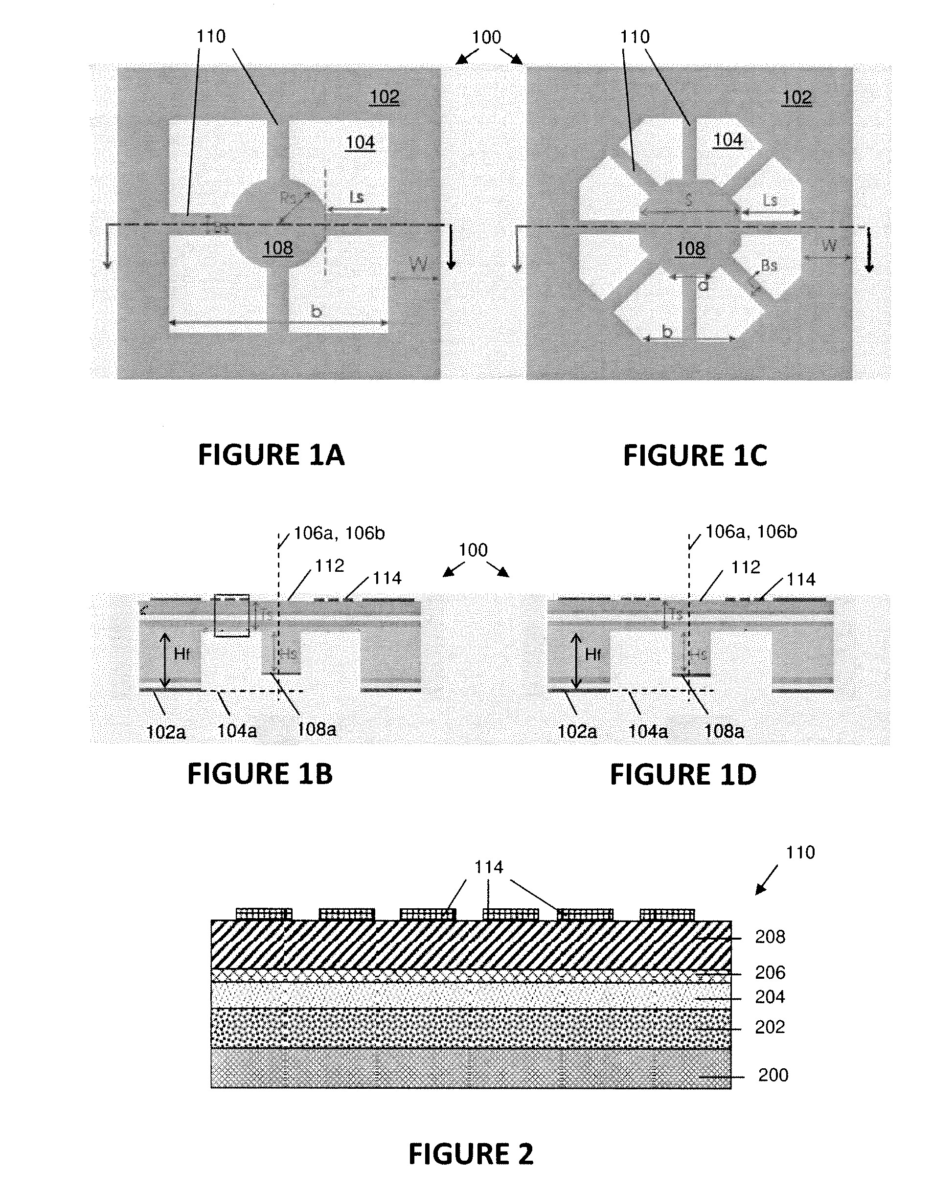
[0050]A double-side polished (DSP) silicon wafer with (100) orientation was used as a base material. SiO2 and SiNx layers were formed on both surfaces of the silicon wafer by thermal oxidation and low pressure chemical vapor deposition (LPCVD) methods, respectively. A yittrium-stabilized zirconia (YSZ) layer was then formed on the SiNx layer on the front side by a sol-gel method. An active piezoelectric sensor material, lead lanthanum zirconium titanate (PLZT) ferroelectric thin film with a thickness of 1.2 μm was prepared by a chemical solution method through a multiple spin-coating process on the YSZ layer. The sample was annealed at 700° C. to form a prevoskite crystalline structure. Inter-digital Au / Ti electrodes were subsequently formed on the PLZT thin film using a lift-off process.

[0051]To define the suspension beam structure and the dicing lines, all the PLZT, YSZ, SiO2 and SiNx layers were etched from the front side with the aid o...

example 2

Micro-Fabrication Process with SOI Wafer

[0056]An SOI wafer is a better wafer option where precise control over the thickness of the suspension beams is desired. In this example, all the thin film deposition processes were similar to those as the normal silicon wafer as described in Example 1. To define the suspension beam structure and the dicing lines, all the PLZT, YSZ, SiO2 and SiNx thin film layers on the front side of the SOI wafer, and the thin Si and insulation SiO2 layers of the SOI wafer, were etched from the front side with the aid of photolithography patterning. For the SOI wafer, the thickness of the Si and SiO2 layers was the desired thickness for the suspension beams, which was about 15 μm in the example (i.e. the thickness of the suspension beams is determined by the thickness of the thin Si layer and the SiO2 layer).

[0057]After the front side processing, a photolithography process was conducted for the patterning at the back side of the wafer. First, a window was ope...


PUM


Abstract

The miniaturized piezoelectric accelerometer includes a support frame (102) having a cavity (104) and a seismic mass (108) supported by a plurality of suspension beams (110) extending from the support frame (102). Each of the suspension beams (110) has a piezoelectric thin film coated on a top surface thereof, with a pair of inter-digital electrodes (114) deposited on an upper surface of each piezoelectric thin film. The presence of acceleration excites bending and thus strain in the piezoelectric thin film, which in turn causes electrical signals to be generated over terminals of the electrodes (114). To collect constructively the output of the electrodes (114), one terminal of each of the electrodes (114) is routed to and electrically connected at a top surface (308) of the seismic mass (108).

Description

FIELD OF THE INVENTION[0001]The present invention relates to miniaturized piezoelectric accelerometers and methods of fabricating miniaturized piezoelectric accelerometers.BACKGROUND OF THE INVENTION[0002]Miniaturized piezoelectric accelerometers are in high demand for applications in aerospace, automobiles, military systems, and machine condition monitoring. Various acceleration sensing mechanisms have been used in accelerometers, including electrostatic, capacitive, piezoresistive, and piezoelectric. Compared to other accelerometers, piezoelectric accelerometers have significant advantages of quick response, high performance at high frequency, high output impedance, low power consumption, and the potential of being self-powered.[0003]Micro electromechanical systems (MEMS) has been applied to produce miniaturized piezoelectric accelerometers using piezoelectric thin films, with the objectives of further miniaturization, improved production consistency, reduced unit cost and the cap...

Claims


Application Information

Patent Timeline
Patent Type & Authority Applications(United States)
IPC IPC(8): G01P15/09H01L41/22G01P15/18
CPCG01P15/0802G01P15/18G01P15/0922G01P2015/084
Inventor YAO, KUISHANMUGAVEL, SARAVANANLUONG, TRUNGDHALIWAL, AJIT S.NG, HON YU PETER
Owner AGENCY FOR SCI TECH & RES
Why Eureka
Try Eureka