

Polarization device, method of manufacturing the same, liquid crystal device, and electronic apparatus
- Summary
- Abstract
- Description
- Claims
- Application Information
AI Technical Summary
Benefits of technology
Problems solved by technology
Method used
Image

Examples
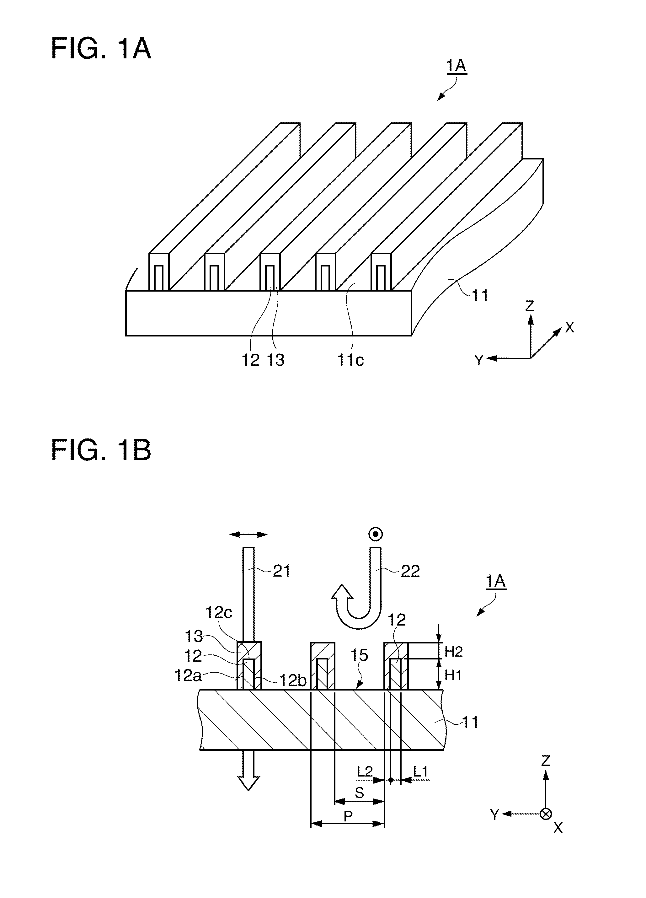
first embodiment
Modified Example of First Embodiment
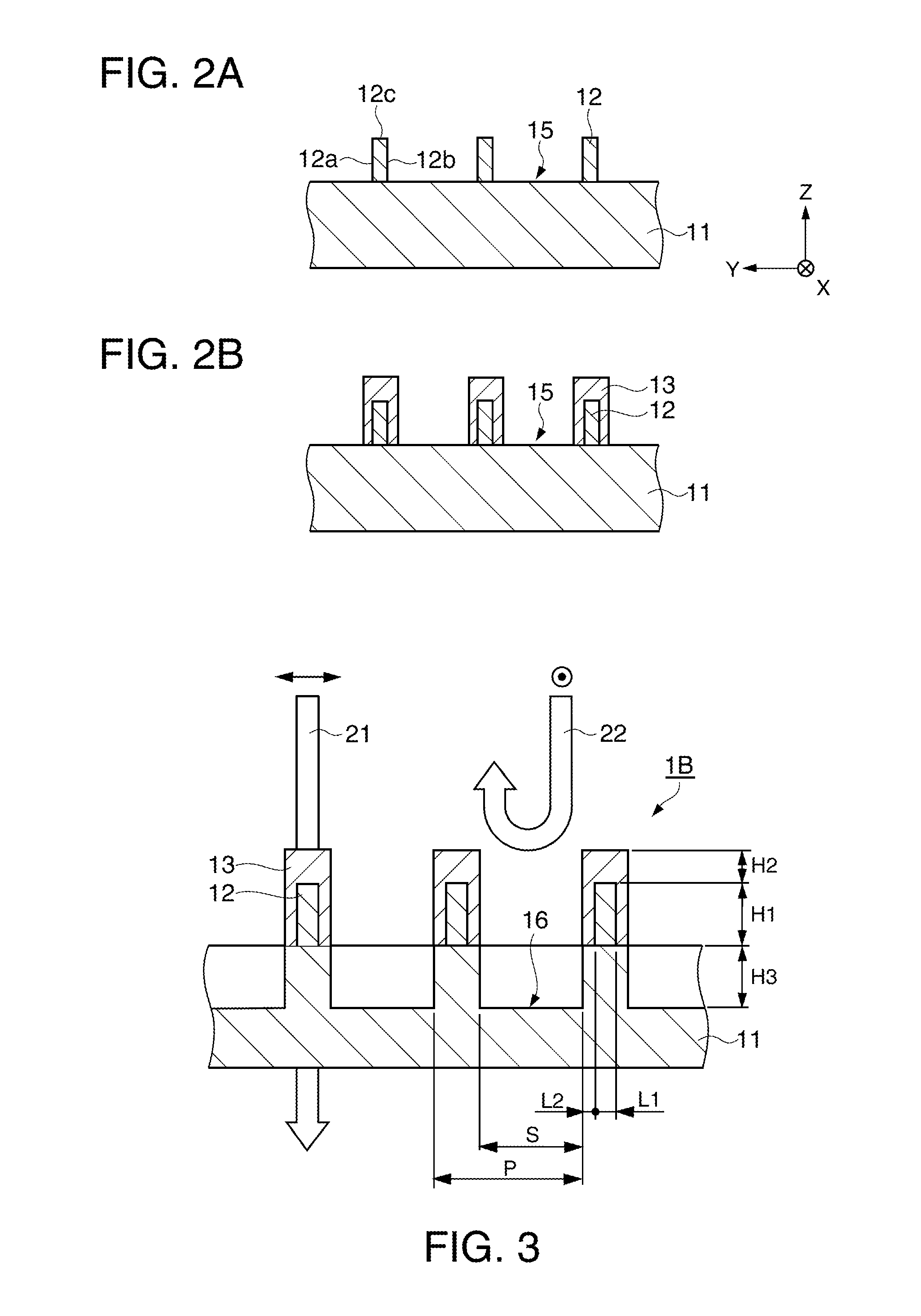
[0054]FIG. 3 shows an explanatory diagram of a polarization device 1B according to a modified example of the first embodiment. The polarization device 1B is partially common with the polarization device 1P, of the first embodiment. There is a difference in that a region 16, which has a refraction index lower than that of the substrate 11, is formed between the metal layers 12.
[0055]As shown in FIG. 3, the polarization device 1B has a region 16 having a refraction index lower than that of the substrate 11 between two adjacent metal layers 12, in addition to the configuration of the polarization device 1A.
[0056]The region 16 is formed by removing the substrate 11 exposed between the two adjacent metal layers 12 through a dry etching or the like. A digging depth H3 is substantially the same as a height H1 of the metal layer 12.
[0057]According to this configuration, it is possible to reduce an effective refraction index of a boundary region between th...
PUM
| Property | Measurement | Unit |
|---|---|---|
| Time | aaaaa | aaaaa |
| Time | aaaaa | aaaaa |
| Time | aaaaa | aaaaa |
Abstract
Description
Claims
Application Information