
Semiconductor package without chip carrier and fabrication method thereof

a technology of semiconductor packaging and chip carrier, which is applied in the direction of semiconductor/solid-state device details, semiconductor devices, electrical apparatus, etc., can solve the problems of poor bonding between the plating layer and the overall thickness of the conventional leadframe qfn semiconductor package, and achieve the effect of reducing manufacturing costs

Active Publication Date: 2012-01-12
SILICONWARE PRECISION IND CO LTD
View PDF3 Cites 22 Cited by
  • Summary
  • Abstract
  • Description
  • Claims
  • Application Information

AI Technical Summary

Benefits of technology

[0008]An objective of the present invention is to provide a semiconductor package without a chip carrier and a fabrication method thereof, which does not require the use of costly Au and Pa as an etching resist layer, thus reduce the manufacturing costs.
[0009]Another objective of the present invention is to provide a semiconductor package without a chip carrier and a fabrication method thereof, which avoids the delamination between a plating layer and an encapsulant.
[0010]A further objective of the present invention is to provide a semiconductor package without a chip carrier and a fabrication method thereof, which avoids the dropping of electrical terminals when requiring rework.
[0011]Still another objective of the present invention is to provide a semiconductor package without a chip carrier and a fabrication method thereof which avoids the bending of copper carrier structure and is helpful to mass-production.
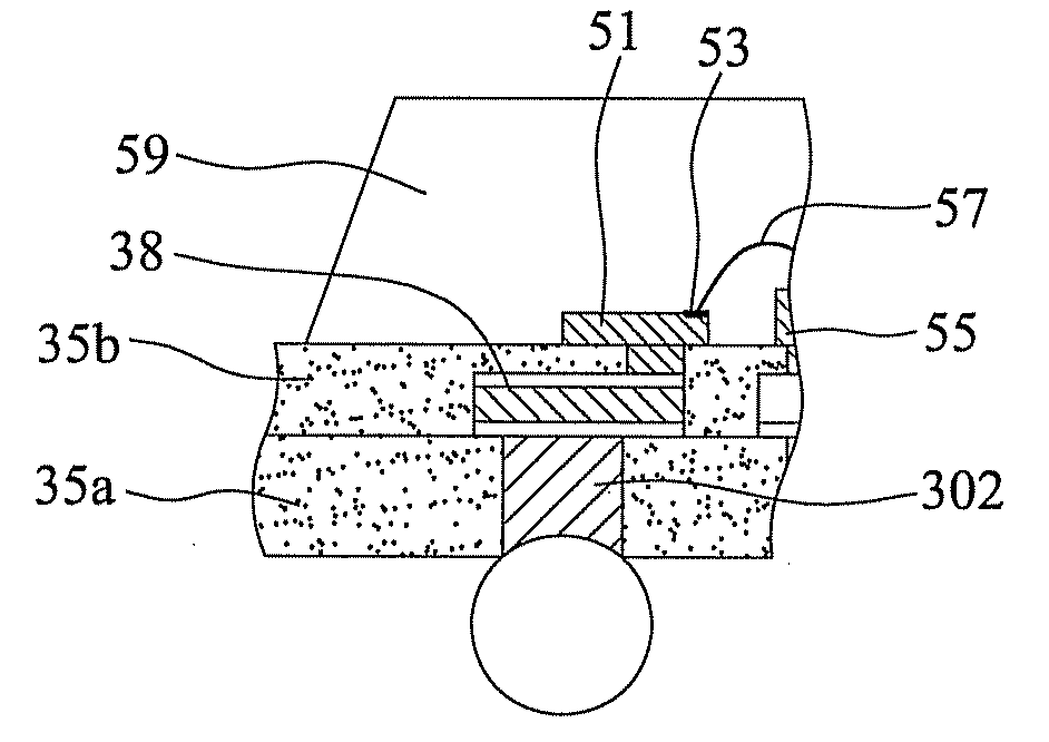
[0013]The semiconductor chip is electrically connected to the bonding pads on the metal studs by flip-chip or wire-bonding techniques. At least one of the bonding pads comprises a metal layer (such as a copper layer) and an anti-oxidant layer that covers the metal layer. The anti-oxidant layer may be a silver layer or an organic solderability preservative (OSP) film. Each of the bonding pads has a cross section greater than a cross section of one of the metal studs on which the bonding pad is formed, such that the bonding pad together with the metal stud form a T-shaped structure. Therefore, the bonding force between the bonding pads and the first encapsulant is enhanced, and the delamination problem is avoided.
[0019]Therefore, the semiconductor package without chip carrier and the fabrication method thereof of the present invention are characterized by forming on a metallic carrier a plurality of grooves and corresponding metal studs by half etching. The metal stud is either an electrical terminal or a die pad. After filling a first encapsulant in the grooves, the first encapsulant is bonded to the metallic carrier via the metal studs directly without the need of spacing other metal material thereinbetween, thereby bonding strength between the first encapsulant and the metallic carrier in enhanced. Subsequently, a bonding pad is formed on each of the metal studs, which comprises a metal layer such as a copper layer and an anti-oxidant layer, such as a silver layer or an OSP film, covering the metal layer. A T-shaped locking structure is thus formed by the bonding pad and the metal stud and securely locked with the first encapsulant, so as to prevent delamination or a moisture penetration from occurrence. As a result, when in need of working the semiconductor package thus fabricated, concerns such as the scrap of the semiconductor package resulting from the drop-off of the terminals and solder joints on the printed circuit board (PCB) from the semiconductor package due to poor bonding between the plating layer and encapsulant. Then, die-mounting, wire-bonding and molding processes, forming a second encapsulant encapsulating a semiconductor chip are sequentially performed, while in the die-mounting, wire-bonding and molding processes, the half-etched grooves are filled with the first encapsulant, so the metallic carrier has a certain structural intension to overcome the drawbacks of having pliable metallic carrier that is difficult for transportation and mass-production as encountered in prior art techniques and, also reduce the manufacturing costs by not requiring the use of the costly metals such as Au and Pd etc. as an etching resist layer.

Problems solved by technology

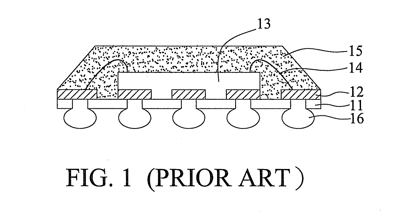
However, with the semiconductor product being striven towards miniaturization continuously, limited by the thickness of an encapsulant, the overall thickness of the conventional leadframe QFN semiconductor package may not be further reduced, therefore the industry has developed a semiconductor package without a chip carrier, which is capable of making overall thickness of the semiconductor package without the chip carrier more light-weight than conventional leadframe QFN semiconductor package.
Furthermore, the manufacturing cost is increased by the use of costly metals such as Au, Pd and the like as an etching resist layer for removing the copper carrier to form the pads 12.
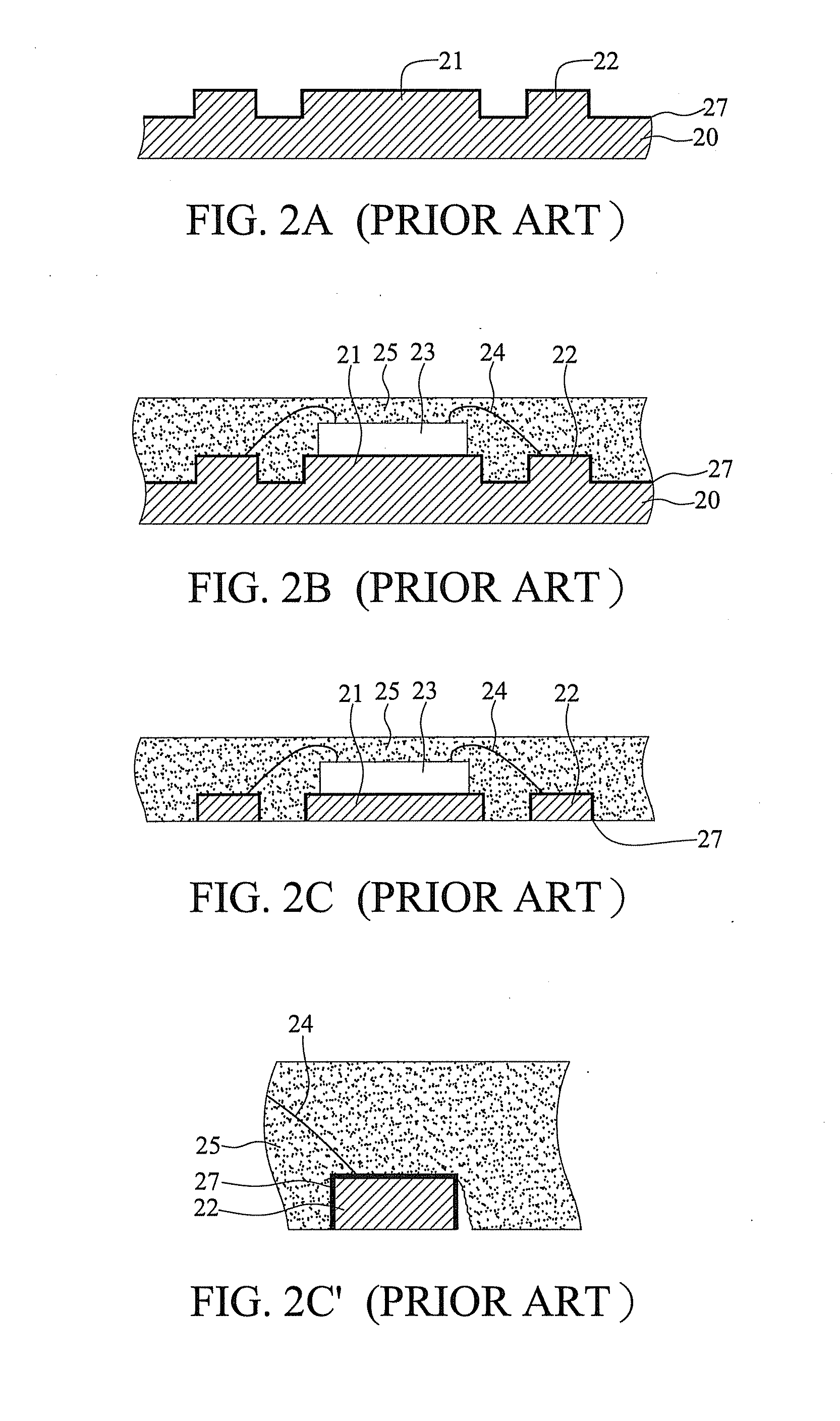
However, there is a poor bonding between the plating layer, such as nickel or silver, and the encapsulant, delamination is caused due to thermal stress, and it further causes moisture penetrating (as shown in FIG.
Furthermore, in the fabrication method, die-mounting, wire-bonding and molding processes should be performed on the half etched copper carrier, because the thickness of the copper carrier is reduced a half so as to make the copper carrier be pliable and thus is difficult for transportation during fabricating, and causes the copper carrier to bend because of heat affecting.
What is more, when I / O terminals of the electrical terminal are increased, bonding wire cross may easily happen because of the design of the pads 22 arranged in an array, thus causing bonding wire short problem.

Method used


Image

  • Semiconductor package without chip carrier and fabrication method thereof
  • Semiconductor package without chip carrier and fabrication method thereof
  • Semiconductor package without chip carrier and fabrication method thereof

Examples


first embodiment

[0028]FIG. 3A to FIG. 3I are diagrams showing a semiconductor package without a chip carrier and a fabrication method thereof according to a first embodiment of the present invention.

[0029]As shown in FIG. 3A, a metallic carrier 30 such as a copper layer is prepared, and the metallic carrier 30 has a first surface 30a and a second surface 30b opposing the first surface 30a.

[0030]As shown in FIG. 3B, a patterned first resist layer 31a is formed on the first surface 30a of the metallic carrier 30. The patterned first resist layer 31a is defined with electrical terminals and the position of die pads. A second resist layer 31b is formed to cover the second surface 30b of the metallic carrier 30. The first resist layer 31a and the second resist layer 31b are, for example, a dry film.

[0031]As shown in FIG. 3C, a part of the metallic carrier 30 uncovered by the first resist layer 31a is removed via a half-etching process, so as to form a plurality of grooves 301 and metal studs 302 corres...

second embodiment

[0045]FIG. 4 is a diagram showing a semiconductor package without a chip carrier and a fabrication method thereof according to a second embodiment of the present invention.

[0046]The present embodiment is substantially similar to the first embodiment, except that a semiconductor chip is electrically connected to the bonding pads on the metal studs by flip-chip technique.

[0047]The semiconductor chip 43 of the present embodiment is mounted on the bonding pads 48 by flip-chip technique. More specifically, the active surface of the semiconductor chip 43 faces the bonding pads 48, and is electrically connected to the bonding pads 48 via a plurality of solder studs 49.

[0048]Compared with the bonding wires that connect the semiconductor chip and the bonding pads, the flip-chip technology using solder studs further shortens the electrical connection path between the semiconductor chip and the bonding pads, and thus it is more capable of ensuring a high quality of the electrical connection be...

third embodiment

[0049]FIG. 5A to FIG. 5C are diagrams showing a semiconductor package without a chip carrier and a fabrication method thereof according to a third embodiment of the present invention.

[0050]The present embodiment is substantially similar to the first embodiment, except that the present embodiment comprises the formation of built-up traces.

[0051]According to the steps of FIG. 3A to FIG. 3F, a plurality of grooves 301 and corresponding metal studs 302 are formed on the metallic carrier 30. After the grooves 301 are filled with the first encapsulant 35a, and the metal studs 302 are exposed from the first encapsulant 35a, a conductive layer 37 such as a thin copper layer is formed on top surfaces of the first encapsulant and the metal studs by electroless plating or sputtering techniques. Then, a patterned third resist layer 31c is formed on the conductive layer 37, and a plurality of openings 310c are formed in the third resist layer 31c to define positions of conductive traces and a di...


PUM


Abstract

A semiconductor package without a chip carrier formed thereon and a fabrication method thereof. A metallic carrier is half-etched to form a plurality of grooves and metal studs corresponding to the grooves. The grooves are filled with a first encapsulant and a plurality of bonding pads are formed on the metal studs. The first encapsulant is bonded with the metal studs directly. Each of the bonding pads and one of the metal studs corresponding to the bonding pad form a T-shaped structure. Therefore, bonding force between the metal studs and the first encapsulant is enhanced such that delamination is avoided. Die mounting, wire-bonding and molding processes are performed subsequently. Since the half-etched grooves are filled with the first encapsulant, the drawback of having pliable metallic carrier that makes transportation difficult to carry out as encountered in prior techniques is overcome, and the manufacturing cost is educed by not requiring the use of costly metals as an etching resist layer.

Description

TECHNICAL FIELD[0001]The present invention relates to semiconductor packaging techniques, and more particularly to a semiconductor package without a chip carrier and a fabrication method thereof.BACKGROUND ART[0002]Conventionally, there are a great variety of semiconductor packages using leadframes as chip carriers, such as quad flat non-leaded (QFN) semiconductor package. The characteristic feature of this QFN semiconductor package is that, unlike a quad flat package (QFP), it does not have external leads being formed outside the package for electrically connecting with external devices, thereby reducing the dimension of the semiconductor packages. However, with the semiconductor product being striven towards miniaturization continuously, limited by the thickness of an encapsulant, the overall thickness of the conventional leadframe QFN semiconductor package may not be further reduced, therefore the industry has developed a semiconductor package without a chip carrier, which is cap...

Claims


Application Information

Patent Timeline
IPC IPC(8): H01L23/48H01L21/56
CPCH01L21/565H01L24/81H01L23/3142H01L24/16H01L24/48H01L2224/16227H01L2224/32225H01L2224/48091H01L2224/48227H01L2224/48235H01L2224/48247H01L2224/484H01L2224/73265H01L2224/81395H01L2224/81439H01L2224/83395H01L2224/83439H01L2224/85001H01L2224/85395H01L2224/85439H01L2924/01028H01L2924/01029H01L2924/01046H01L2924/01078H01L2924/01079H01L2924/15311H01L21/568H01L24/11H01L21/486H01L2224/16225H01L2924/00014H01L2224/45099H01L2924/00H01L2924/351H01L2924/15747H01L2924/181H01L23/3135H01L23/3114H01L2924/00012H01L2224/45015H01L2924/207
Inventor TSAI, YUEH-YINGTANG, FU-DIHUANG, CHIEN-PINGKE, CHUN-CHI
Owner SILICONWARE PRECISION IND CO LTD
Learn More