Method for Wafer Dicing and Composition Useful Thereof

Active Publication Date: 2012-01-12
VERSUM MATERIALS US LLC
View PDF14 Cites 12 Cited by
  • Summary
  • Abstract
  • Description
  • Claims
  • Application Information

AI Technical Summary

Benefits of technology

[0006]It is therefore an objective of the present invention to provide a dicing solution or a solution for semiconductor wafer dicing, and a method to use the solu

Problems solved by technology

They are difficult to remove in subsequent cleaning processes once in contact with wafer and virtually impossible to remove once trapped in deep trenches.
In addition, during the dicing process, the bonding pads are exposed for corrosion to occur.
Corrosion can damage the bonding pads leading to poor bonding performance, poor reliability, or even failure of the device.
The contaminant particles and corrosion can cause

Method used


Image

  • Method for Wafer Dicing and Composition Useful Thereof
  • Method for Wafer Dicing and Composition Useful Thereof
  • Method for Wafer Dicing and Composition Useful Thereof

Examples


working examples

Group I

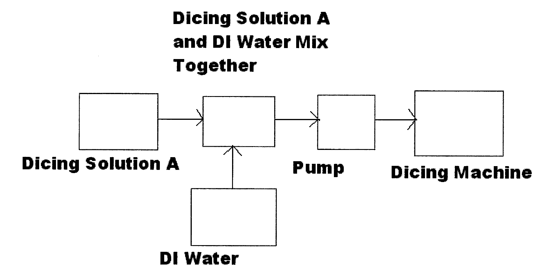
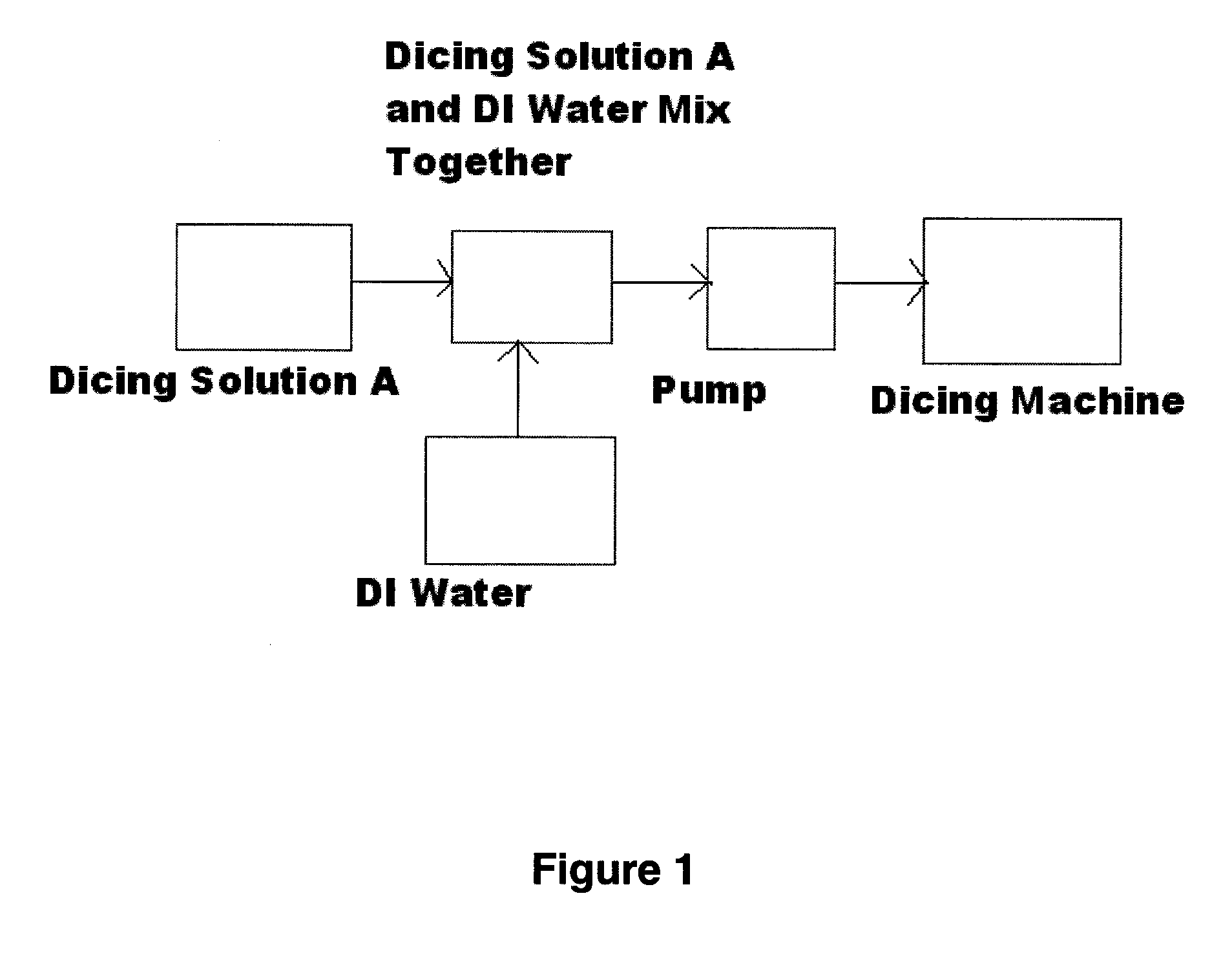
[0066]A dicing solution 38A comprising water (95.28 wt %), citric acid (2 wt %), potassium hydroxide(KOH)(0.72 wt %), and Tergitol 15-S-7 (2 wt %) was made.

[0067]A dicing solution 38B comprising water (>90 wt %), Hostapur SAS (1 wt %), Dynol 604 (0.5 wt %), citric acids (2 wt %) and potassium hydroxide (KOH) (<7.5 wt %) to adjust pH to 6 was made similarly as for the dicing solution 38A.

[0068]A dicing solution 38C comprising water (>90 wt %), Triton X-100 (2 wt %), Citric acid (2 wt %), and potassium hydroxide (KOH) (<6 wt %) to adjust pH to 6 was made similarly as for the dicing solution 38A.

[0069]A dicing solution 38D comprising water (>90 wt %), ethylene diaminetetraacetic acid (2 wt %), Tergitol 15-S-7 (2 wt %), and tetraethylammonium hydroxide(<6 wt %) to adjust pH to 7 was made similarly as for the dicing solution 38A.

[0070]A dicing solution 38E comprising water (>90 wt %), glycine (2 wt %), and Tergitol 15-S-7 (2 wt %) was made similarly as for the dicing solution 38A....

example 3

[0098]Al(0.5% Cu) metal on titanium nitride (TiN) substrate with a resistivity of 338.24 ohms-Å / Sq was obtained from SVMI and had nominally 8000 Å thickness of Al. During storage the Al substrate can grow up to 150 Å of an oxide layer. Prior to etch rate determinations the Al substrate was therefore pretreated by immersing a 2″×2″ piece of Al into an aqueous solution of 42.5 wt % H3PO4 in de-ionized water for 2 minutes at 25° C. After immersing for 2 minutes, the Al piece was rinsed for 3 minutes with de-ionized water, dried with a N2 gun for 30 seconds, and the Al film thickness was then measured. Al pieces pretreated in this way were used immediately in etch rate measurements performed.

example 4

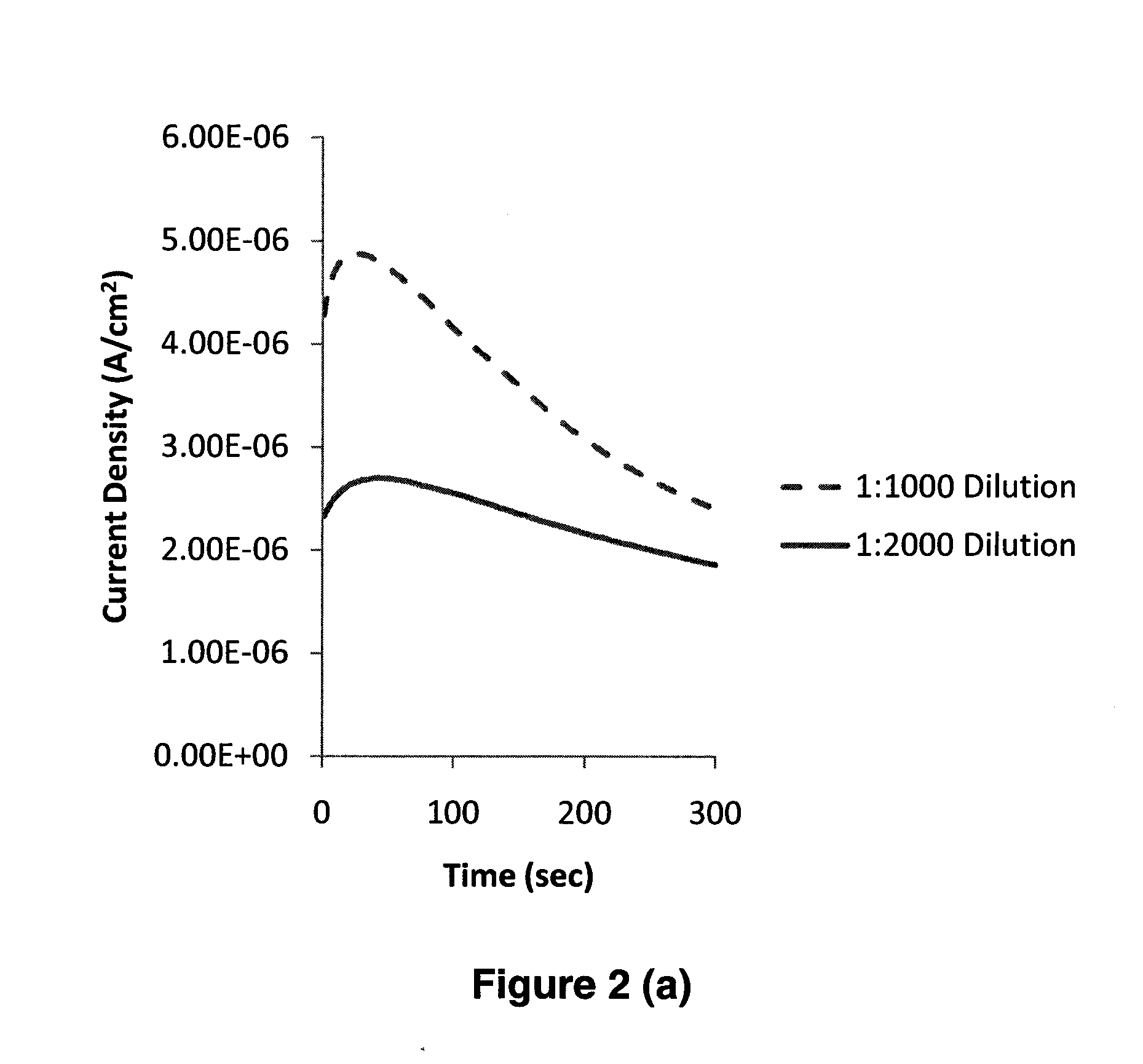
[0099]A dicing solution comprising 2.0 wt % oxalic acid in de-ionized water was prepared as follows: To a one liter HDPE poly-bottle was added 224.2 gm of an aqueous solution containing 8.92 wt % oxalic acid. An additional 775.8 gm of de-ionized water was then added to the bottle to a final weight of 1000.0 gm. The bottle was capped and shaken. The dicing solution was named 48A and the solution pH was measured to be 1.04.

[0100]Dicing solution 48A was submitted for etch rate measurements at 25° C. using a pretreated piece of Al, as well as using 1000 Å Ni on thermal oxide (TOx) substrates. The Ni substrate had a resistivity of 2035.64 ohm-Å / Sq. Each 2″×2″ piece of Al or Ni substrate was immersed into 330 ml of the 48A dicing solution in a 500 ml glass beaker and the solution stirred on a stir plate at 300 rpm. The temperature was recorded. Thickness measurements in Å were made in triplicate after times 0, 20, 40, 60, and 90 minutes using a ResMap Four Point probe. The film thickness ...


PUM

PropertyMeasurementUnit
Timeaaaaaaaaaa
Fractionaaaaaaaaaa
Fractionaaaaaaaaaa

Abstract

A solution for semiconductor wafer dicing is disclosed. The solution suppresses the adherence of contamination residues or particles, and reduces or eliminates the corrosion of the exposed metallization areas, during the process of dicing a wafer by sawing. The solution comprises at least one organic acid and/or salt thereof; at least a surfactant and/or at least a base; and deionized water, the composition has a pH is equal or greater than 4. The solution can further comprise, a chelating agent, a defoaming agent, or a dispersing agent.

Description

CROSS-REFERENCE TO RELATED APPLICATIONS[0001]This application claims the benefit of priority under 35 U.S.C. §119(e) to earlier filed U.S. provisional patent application Ser. No. 61 / 362,896, filed on Jul. 7, 2010, the disclosure of which is incorporated herein by reference in its entirety.BACKGROUND OF THE INVENTION[0002]The integrated circuits are usually formed on a wafer. A single wafer contains plurality of integrated circuit chips, or dies. An integrated circuit chip or dice, is obtained through a dicing process of sawing the wafer.[0003]During the dicing process, small contaminant residues / particles from sawing the wafer, usually silicon residue, adhere to wafer surface, accumulate in bonding pads and trenched locations. They are difficult to remove in subsequent cleaning processes once in contact with wafer and virtually impossible to remove once trapped in deep trenches. In addition, during the dicing process, the bonding pads are exposed for corrosion to occur. Corrosion ca...

Claims


Application Information

Patent Timeline
IPC IPC(8): H01L21/78C23F11/14C23F11/167C23F11/12
CPCB28D5/0076C11D3/044H01L2224/94C11D3/2075C11D3/30C11D3/33C11D11/0047C11D3/2082H01L21/67075H01L21/78H01L21/02076H01L2224/0381H01L2224/04042H01L2224/05624H01L2224/05647H01L2224/03H01L21/30C11D1/14
Inventor TAMBOLI, DNYANESH CHANDRAKANTRAMAMURTHI, RAJKUMARRENNIE, DAVID BARRYRAO, MADHUKAR BHASKARABANERJEE, GAUTAMPARRIS, GENE EVERAD
Owner VERSUM MATERIALS US LLC
Why Eureka
Try Eureka