Ultraviolet light emitting diode devices and methods for fabricating the same

a technology of ultra-violet light and diodes, which is applied in the field of ultra-violet light emitting diodes, can solve the problems of difficult fabrication of high-quality algan materials, low external quantum efficiency and light power of ultra-violet led devices, and increase the active composition of gan-based led devices, etc., to facilitate the practical application of algan-based ultra-violet led devices. , the effect of improving the aperture of light emission

Inactive Publication Date: 2012-01-26
XIDIAN UNIV
View PDF0 Cites 26 Cited by
  • Summary
  • Abstract
  • Description
  • Claims
  • Application Information

AI Technical Summary

Benefits of technology

[0014]Since the device according present invention has a top window structure, not only the light emission aperture is improved, but also the light emission from the window is enhanced. Even defects in the AlN buffer layer of the device are increased due to electric stress, the power of light emission would not be influenced, which would facilitate the practical application of AlGaN-based UV LED device with SiC substrate.
[0015]In addition, in the fabrication of the top window structure, the semi-sphere, cone, etc. shape windows are formed by wet etching the p-GaN cap layer to the p-type AlGaN barrier layer with the aid of light, so that the UV light emitted can exit from the top, and light emission power and external quantum efficiency of the device can be improved.
[0016]Furthermore, in present invention, the window is formed by a dry etching, so that the surface of the electronic barrier layer p-AlGaN at bottom of the window is roughened, and the light emission efficiency is further improved.
[0017]Also, according to present invention, the process for fabricating the device is fully compatible with the mature process for fabricating the blue-light GaN based LED devices, thereby the cost is low and the process is simple.

Problems solved by technology

However, as the wavelength of light emitted from the LED devices becomes shorter, Al composition in active layer of the GaN-based LED devices is increasingly high.
Therefore, it is difficult to fabricate a high quality AlGaN material.
Particularly, the external quantum efficiency and the light power of the UV LED devices are very low because the AlGaN material absorbs UV light strongly, which have become a bottleneck for developing the UV LED devices and a problem to be solved currently.
However, due to the bottom emission type, the emission efficiency was still low, referring to V. Adivarahan, W. H. Sun, A. Chitnis, M. Shatalov, S. Wu, H. P. Maruska, M. Asif. Khan. “250 nm AlGaN light-emitting diodes” Appl. Phys. Lett, 2004, 85 (12):2175.
With decrease of the emission wavelength, the bottom buffer layer absorbs UV light increasingly, thereby producing an adverse effect on the light emission power and external quantum efficiency.
However, existing bottom emission type LED devices have following disadvantages: first, the emission path of light is too long and light loss on the path is too large, causing the external quantum efficiency to be low.
Secondly, the crystallizing quality of bottom AlN buffer layer is poor, thereby causing increased non-radiative recombination centers in the material and increased UV light being absorbed.
Thirdly, there are increased defects of trapping photons in the bottom buffer layer under electrical stress, adversely affecting the reliability of the devices.

Method used


Image

  • Ultraviolet light emitting diode devices and methods for fabricating the same
  • Ultraviolet light emitting diode devices and methods for fabricating the same
  • Ultraviolet light emitting diode devices and methods for fabricating the same

Examples


first embodiment

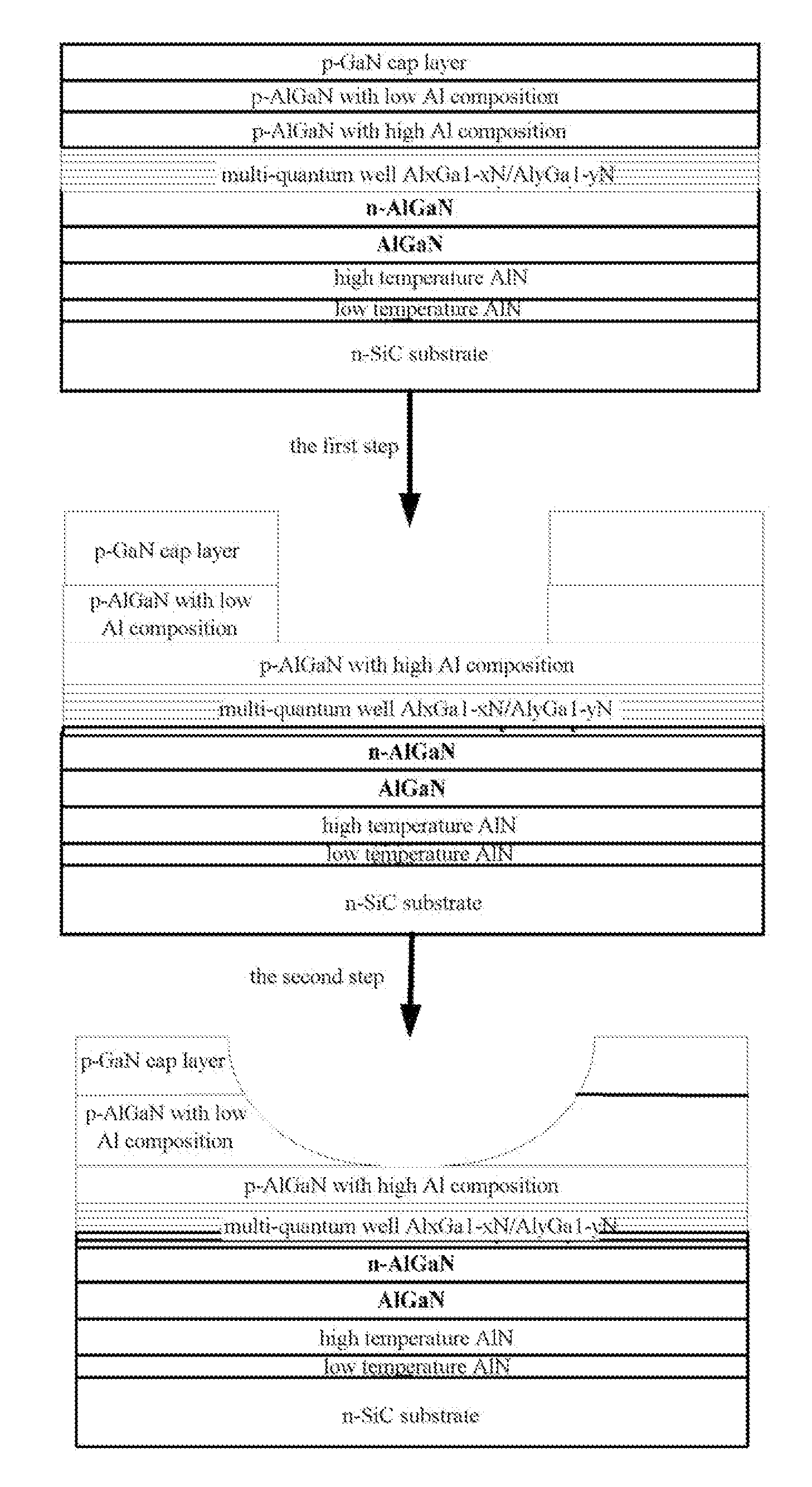
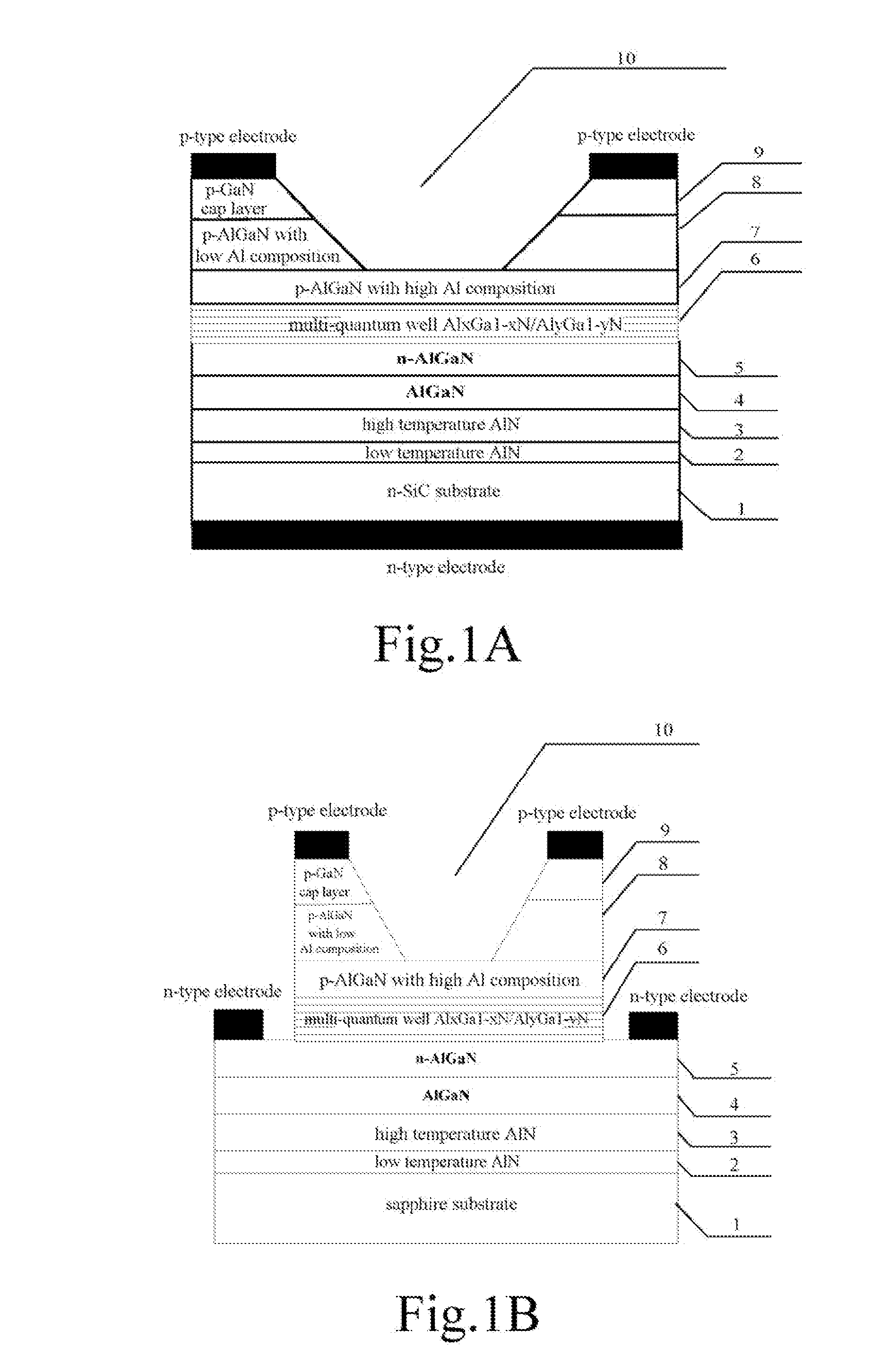
[0035]Hereinafter, a method for fabricating the UV LED device shown in FIG. 1E having a SiC substrate and a cylindrical window, is described with respect to FIGS. 2A and 2B.

[0036]First, a material growth step is shown is FIG. 2A:

[0037]At step 1, on the SiC substrate, a low-temperature AlN nucleating layer is grown by a MOCVD process.

[0038]Lowering a temperature of the substrate to 600° C.; retaining a growing pressure of 50 Torr, a flow rate of 1500 sccm of hydrogen gas, a flow rate of 1500 sccm of ammonia gas; introducing an Al source at a flow rate of 28 μmol / min into a reaction chamber; and growing the low-temperature AlN nucleating layer with a thickness of 3 nm.

[0039]At step 2, on the low-temperature AlN nucleating layer, a high-temperature AlN nucleating layer is grown.

[0040]Raising a growing temperature to 1050° C.; retaining the growing pressure of 50 Torr, the flow rate of 1500 sccm of hydrogen gas, the flow rate of 1500 sccm of ammonia gas; introducing the Al source at a f...

second embodiment

[0079]Hereinafter, a method for fabricating the UV LED device shown in FIG. 1F, having a sapphire substrate and a cylindrical window, is described with respect to FIGS. 3A-3C.

[0080]First, a material growth step is shown is FIG. 3A:

[0081]At step 1, on the sapphire substrate, a low-temperature AlN nucleating layer is grown using a MOCVD process.

[0082]Lowering a temperature of the substrate to 600° C.; retaining a growing pressure of 50 Torr, a flow rate of 1500 sccm of hydrogen gas, a flow rate of 1500 sccm of ammonia gas; introducing an Al source at a flow rate of 28 μmol / min into a reaction chamber; and growing the low-temperature AlN nucleating layer with a thickness of 5 nm.

[0083]At step 2, on the low-temperature AlN nucleating layer, a high-temperature AlN nucleating layer is grown.

[0084]Raising a growing temperature to 1050° C.; retaining the growing pressure of 50 Torr, the flow rate of 1500 sccm of hydrogen gas, the flow rate of 1500 sccm of ammonia gas; introducing the Al sou...

third embodiment

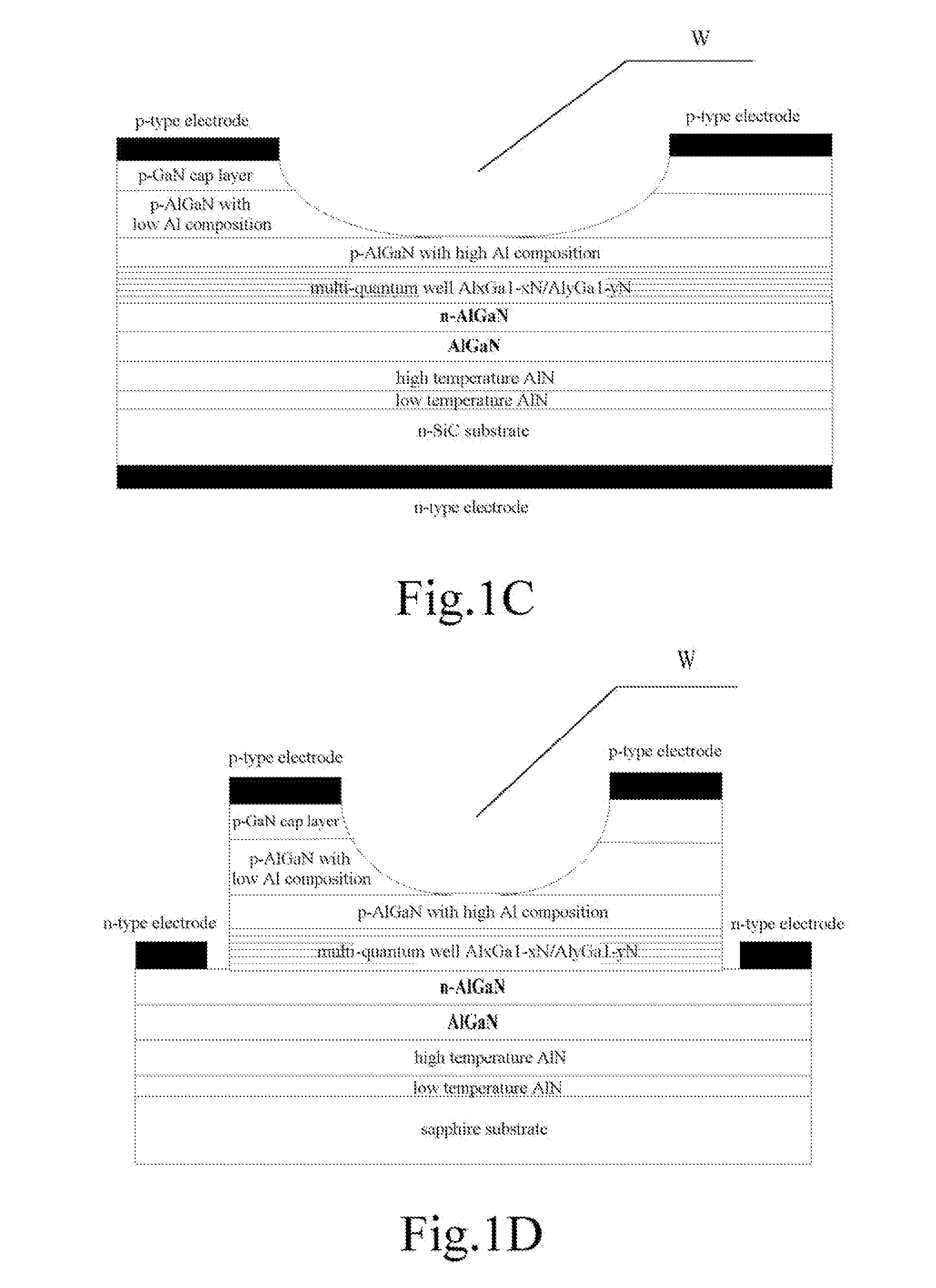
[0128]Hereinafter, a method for fabricating the UV LED device shown in FIG. 1A, having a SiC substrate and a conic window, is described with respect to FIG. 4. On the SiC substrate 1, a cone-like window is made using the ICP dry etching and a wet etching, the steps are as follows.

[0129]At step 1, on the SiC substrate 1, a low-temperature AlN nucleating layer 2 is grown using the MOCVD process.

[0130]Lowering a temperature of the substrate to 600° C.; retaining a growing pressure of 50 Torr, a flow rate of 1500 sccm of hydrogen gas, a flow rate of 1500 sccm of ammonia gas; introducing an Al source at a flow rate of 28 μmol / min into a reaction chamber; and growing the low-temperature AlN nucleating layer with a thickness of 10 nm.

[0131]At step 2, on the low-temperature AlN nucleating layer 2, a high-temperature AlN nucleating layer 3 is grown.

[0132]Raising a growing temperature to 1050° C.; retaining the growing pressure of 50 Torr, the flow rate of 1500 sccm of hydrogen gas, the flow ...


PUM

PropertyMeasurementUnit
pressureaaaaaaaaaa
bias voltageaaaaaaaaaa
temperatureaaaaaaaaaa

Abstract

A UV LED device and the method for fabricating the same are provided. The device has aluminum nitride nucleating layers, an intrinsic aluminum gallium nitride epitaxial layer, an n-type aluminum gallium nitride barrier layer, an active region, a first p-type aluminum gallium nitride barrier layer, a second p-type aluminum gallium nitride barrier layer, and a p-type gallium nitride cap layer arranged from bottom to top on a substrate. A window region is etched in the p-type gallium nitride cap layer for emitting the light generated.

Description

TECHNICAL FIELD[0001]The present invention relates to light emitting diode (hereinafter referred to as “LED”) devices and methods for fabricating the same, and more particularly, to AlGaN-based multi-quantum well ultraviolet (UV) LED devices with improved light emission intensity and methods for fabricating the same.BACKGROUND OF THE INVENTION[0002]Group III-V compound semiconductor materials which are representative of the third generation semiconductor materials have many excellent properties, and particularly in terms of optical application, alloys {Ga(Al, In)N} consisting of Ga, Al, In and N may be suitable for both the visible light region and the near-UV light region. Furthermore, group III nitrides having wurtzite structure are of direct band gap and very suitable for photoelectronic device application. AlGaN-based multi-quantum well UV LED devices, as a focus of current UV photoelectronic device development, have exhibited great advantages especially for UV light region. How...

Claims


Application Information

Patent Timeline
Patent Type & Authority Applications(United States)
IPC IPC(8): H01L33/40H01L33/32
CPCH01L33/20H01L33/06
Inventor HAO, YUEYANG, LINGMA, XIAOHUAZHOU, XIAOWEILI, PEIXIAN
Owner XIDIAN UNIV
Why Eureka
Try Eureka