Gas barrier film and electronic device
a technology of gas barrier film and electrode film, which is applied in the direction of metallic material coating process, synthesizing resin layered products, record information storage, etc., can solve the problems of disconnections or short circuits in electrode films, poor gas barrier properties of transparent resin films, and inability to adequately prevent water vapor entry, etc., to achieve high surface flatness, facilitate handling, inhibit layer separation
- Summary
- Abstract
- Description
- Claims
- Application Information
AI Technical Summary
Benefits of technology
Problems solved by technology
Method used
Image
Examples
example 1
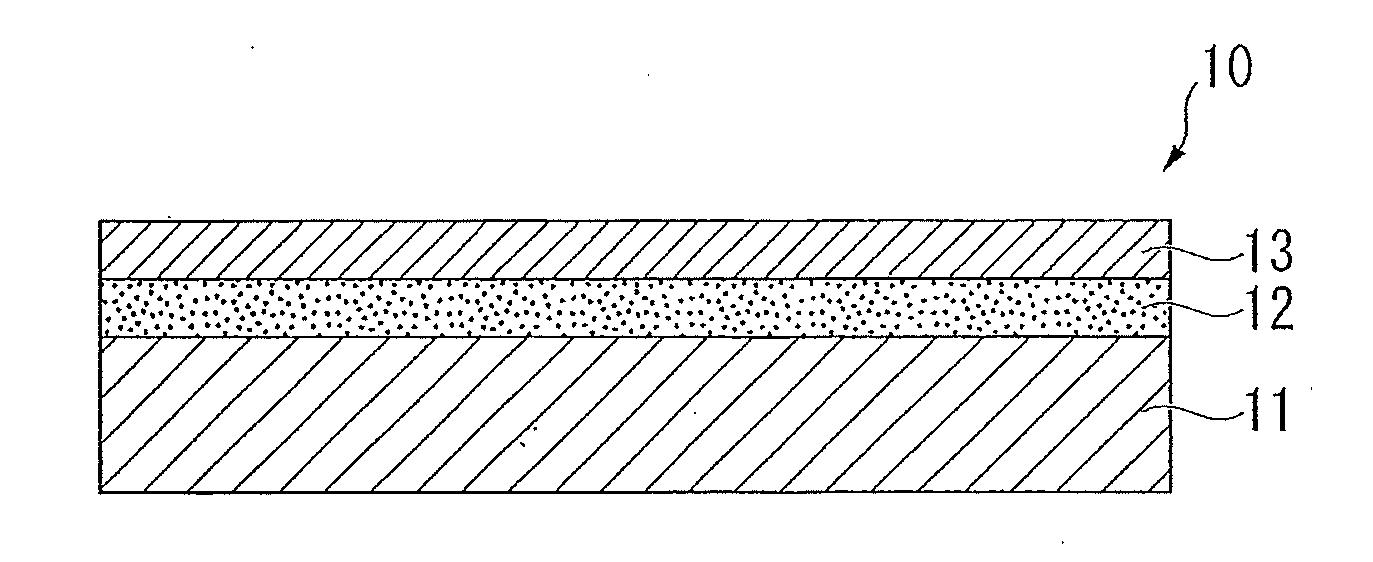
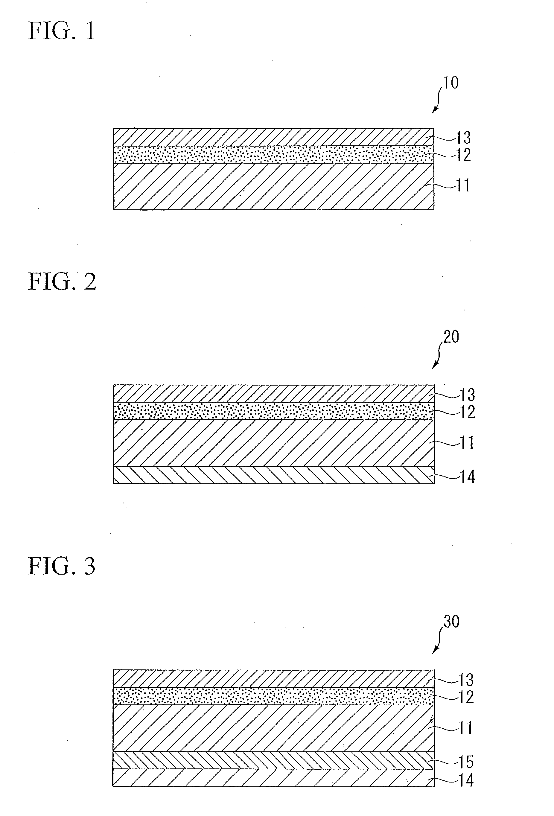
[0136]A polyethylene terephthalate film (produced by Mitsubishi Plastics, Inc., trade name: PET38 T-100) having a thickness of 38 μm was prepared for use as a base.
[0137]Next, a silicone resin (produced by Shin-Etsu Chemical Co., Ltd., trade name: KS847H), mainly composed of polydimethylsiloxane for the polyorganosiloxane-based compound, was coated onto the surface of the base and dried to obtain a polydimethylsiloxane layer (polyorganosiloxane layer) having a thickness of 100 nm.
[0138]Next, a silicon nitride (Si—N) film (inorganic material layer) was deposited on the polydimethylsiloxane layer by dynamic ion mixing method using a sputtering method.
[0139]The conditions of dynamic ion mixing method are indicated below.
[0140]Plasma-forming gas: Mixed gas of argon and nitrogen
[0141]Target: Silicon
[0142]Plasma-forming gas flow rates: argon: 100 cm3 / min (atmospheric pressure: 1.013 hPa, 25° C.), nitrogen: 60 cm3 / min (atmospheric pressure 1.013 hPa, 25° C.)
[0143](Radio Frequency Electrica...
example 2
[0155]A gas barrier film was produced in the same manner as Example 1 with the exception of using a mixed gas of argon and oxygen for the plasma-forming gas when forming the inorganic material layer, and depositing a silicon oxide (SiO2) film by setting the argon flow rate to 100 sccm and setting the oxygen flow rate to 30 sccm.
example 3
[0156]A gas barrier film was produced in the same manner as Example 1 with the exception of depositing an aluminum nitride (Al—N) film by using aluminum for the target when forming the inorganic material layer.
PUM
| Property | Measurement | Unit |
|---|---|---|
| voltage | aaaaa | aaaaa |
| thickness | aaaaa | aaaaa |
| thickness | aaaaa | aaaaa |
Abstract
Description
Claims
Application Information


