Liquid Crystal Display Device

a liquid crystal display and display device technology, applied in non-linear optics, instruments, optics, etc., can solve the problems of low reliability at a high temperature, low aperture ratio of every pixel, etc., and achieve high definition, good temperature characteristics, and improved light incidence efficiency

Inactive Publication Date: 2012-02-09
SEMICON ENERGY LAB CO LTD
View PDF4 Cites 20 Cited by
  • Summary
  • Abstract
  • Description
  • Claims
  • Application Information

AI Technical Summary

Benefits of technology

[0019]In the liquid crystal display device, an optical member may be provided between the pair of substrates and the light guide member included in the lighting portion in order to improve the efficiency of incidence of light on the pixel portion including a liquid crystal element, the luminance of an image displayed on the pixel portion, and the like.
[0020]According to one embodiment of the present invention, a liquid crystal display device having high definition and good temperature characteristics in which color change can be corrected can be provided. In addition, owing to the good temperature characteristics, a liquid crystal display device which is suitable for outdoor use can be provided.

Problems solved by technology

However, it is necessary that the conventional semi-transmissive liquid crystal display device be provided with a light-transmitting pixel electrode for a transmissive type and provided with a reflective pixel electrode for a reflective type, which causes a low aperture ratio of every pixel.
In particular, the electrical characteristics of an amorphous silicon thin film transistor (TFT), which is widely used in an active matrix liquid crystal display device, vary at a high temperature, which causes low reliability at a high temperature.

Method used


Image

  • Liquid Crystal Display Device
  • Liquid Crystal Display Device
  • Liquid Crystal Display Device

Examples


embodiment 1

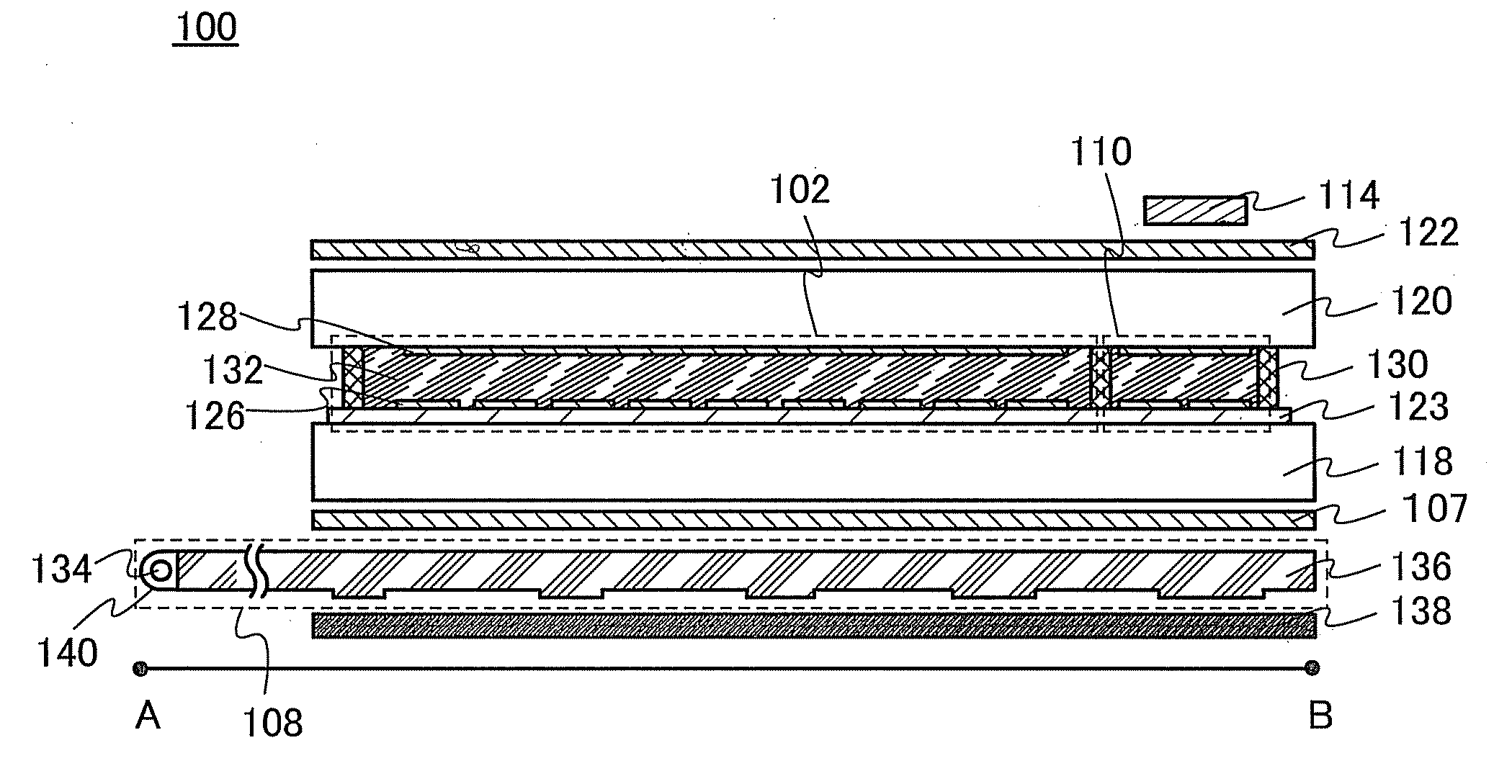
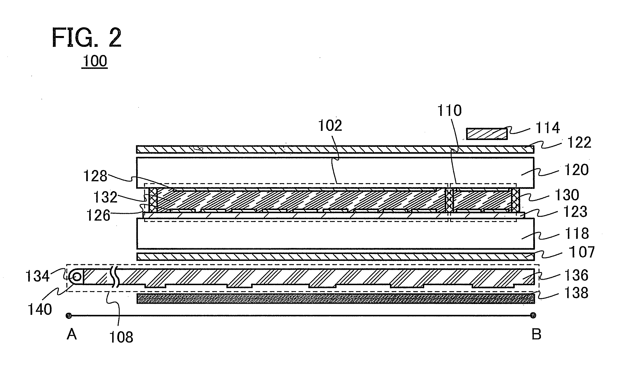
[0041]In this embodiment, a liquid crystal display device 100 that is one embodiment of the present invention will be described with reference to FIGS. 1A and 1B, FIG. 2, FIGS. 3A to 3D, FIGS. 4A and 4B, and FIGS. 5A and 5B.

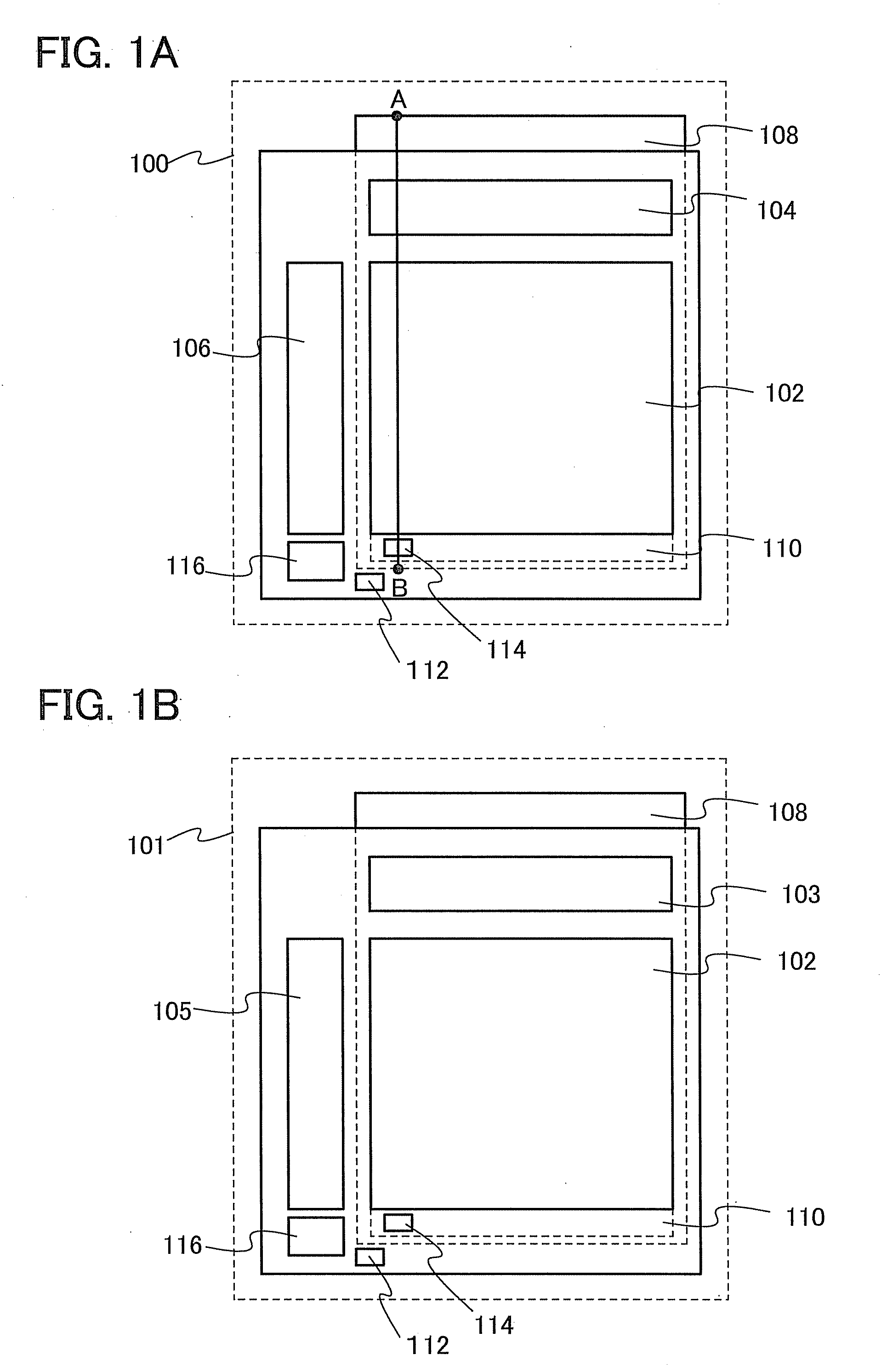
[0042]A liquid crystal display device (mainly, a pixel portion) that is one embodiment of the present invention can be applied to either a passive matrix type or an active matrix type. FIG. 1A is a block diagram illustrating a structure of an active matrix type, and FIG. 1B is a block diagram illustrating a structure of a passive matrix type.

[0043]In FIG. 1A, the liquid crystal display device 100 of an active matrix type includes, over a substrate, a pixel portion 102, a signal line driver circuit 104, a scan line driver circuit 106, a lighting portion 108 that makes light incident on the pixel portion 102, a monitoring pixel portion 110, a first optical sensor 112 that detects the illuminance of external light, a second optical sensor 114 that detects a change i...

embodiment 2

[0129]In this embodiment, a transistor 430 provided in a liquid crystal display device 100 of an active matrix type and included in a transistor element layer 123 will be described (see FIG. 4B). Note that the transistor 430 is an inverted-staggered thin film transistor.

[0130]The transistor element layer 123 includes a transistor operated even at high temperature or the like, that is, having good temperature characteristics, and thus a semiconductor including a plurality of crystal regions is used as a semiconductor layer 408 of the transistor 430. As the semiconductor including a plurality of crystal regions, a microcrystalline silicon semiconductor, a polycrystalline silicon semiconductor, or the like is used. Further, not only a silicon semiconductor but also a germanium semiconductor may be used. Furthermore, an oxide semiconductor can also be used. Note that an oxide semiconductor refers to a metal oxide having semiconductor characteristics here. In this embodiment, manufacturi...

embodiment 3

[0197]In this embodiment, a manufacturing method of a thin film transistor which has a different structure from the thin film transistor described in Embodiment 2 is described with reference to FIGS. 6A to 6D, FIGS. 8A to 8C and FIG. 10. FIG. 10 corresponds to the step illustrated in FIG. 8B.

[0198]In a manner similar to Embodiment 2, through the processes illustrated in FIGS. 6A to 6D and FIG. 8A, a conductive film 127 is formed.

[0199]Then, as illustrated in FIG. 10, a source electrode 405a and a drain electrode 405b are formed and an impurity semiconductor film 121 and a semiconductor stack 117 are partly etched, so that pair of impurity semiconductor films 131a and 131b serving as a source region and a drain region is formed as in Embodiment 2. In addition, a semiconductor stack 143 including a microcrystalline semiconductor region 143a and an amorphous semiconductor region 143b is formed. At this time, by etching the semiconductor stack 117 so that the amorphous semiconductor reg...


PUM

PropertyMeasurementUnit
sizesaaaaaaaaaa
sizesaaaaaaaaaa
sizesaaaaaaaaaa

Abstract

A liquid crystal display device which includes a pair of substrates, a pixel including a liquid crystal element between the pair of substrates, a lighting portion provided on the outer side of the pair of substrates, a first polarizing member between the pair of substrates and the lighting portion, a reflective member provided outside the lightning portion, a second polarizing member on a side opposite to the first polarizing member with the pair of substrates provided therebetween, and a first optical sensor and a second optical sensor. The first optical sensor has a function of detecting illuminance of external light, and the second optical sensor has a function of detecting a color tone of polarized light emitted from the pixel portion. The lightning portion can emits light having a predetermined wavelength depending on the color tone of the pixel portion which is detected by the second optical sensor.

Description

BACKGROUND OF THE INVENTION[0001]1. Field of the Invention[0002]The present invention relates to a liquid crystal display device and a method for manufacturing the liquid crystal display device.[0003]2. Description of the Related Art[0004]Liquid crystal display devices for outdoor use, such as digital signage, have been developed.[0005]As a liquid crystal display device suitable for outdoor use, for example, a reflective liquid crystal display device that displays an image with the use of external light, and further, a liquid crystal display device that is obtained by adding a side light to a reflective liquid crystal display device so that display of an image can be performed even in the situation where external light is insufficient are given (see Patent Document 1).[0006]In addition, a semi-transmissive liquid crystal display device which functions as a reflective liquid crystal display device in the case with external light, and functions as a transmissive liquid crystal display...

Claims


Application Information

Patent Timeline
Patent Type & Authority Applications(United States)
IPC IPC(8): G02F1/1335
CPCG02F1/133555G02F2201/58G02F2001/133618G02F1/133615G02F1/133618
Inventor YAMAZAKI, SHUNPEITORIUMI, SATOSHIISA, TOSHIYUKI
Owner SEMICON ENERGY LAB CO LTD
Why Eureka
Try Eureka