Semiconductor device and manufacturing method thereof

a technology of semiconductor devices and manufacturing methods, applied in the direction of semiconductor devices, resistors, electrical devices, etc., can solve the problems of reducing the gate capacitance, reducing the current driving capability, and reducing so as to improve the reliability of the misfet

Inactive Publication Date: 2012-03-08
RENESAS ELECTRONICS CORP
View PDF3 Cites 14 Cited by
  • Summary
  • Abstract
  • Description
  • Claims
  • Application Information

AI Technical Summary

Benefits of technology

[0018]In a semiconductor device having a MISFET using an insulating film containing hafnium

Problems solved by technology

On the other hand, when the thickness of the gate insulating film is increased to reduce the leakage current in the MISFET, the gate capacitance decreases to reduce the current driving capability.
However, the insulating film containing hafnium has the problem that a large number of fixed charges and trap levels are formed therein, and degrade the reliability of the MISFET.
In particular, a

Method used


Image

  • Semiconductor device and manufacturing method thereof
  • Semiconductor device and manufacturing method thereof
  • Semiconductor device and manufacturing method thereof

Examples


first embodiment

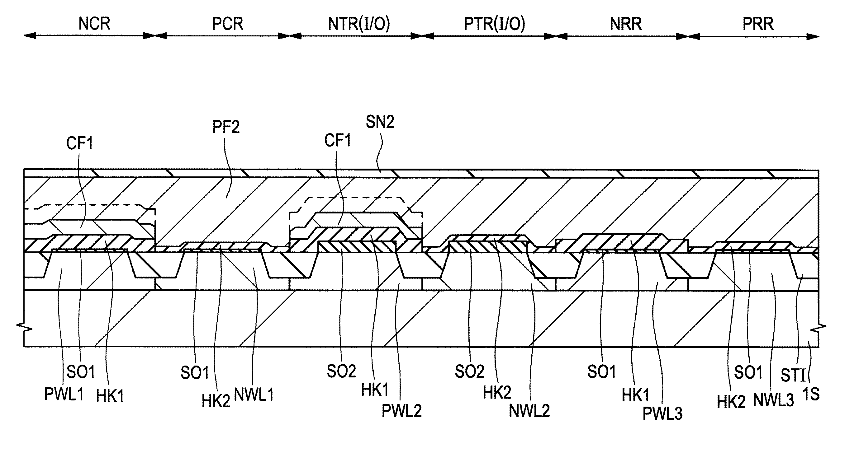
[0071]A semiconductor device in the present first embodiment will be described with reference to the drawings. First, a description will be given to a layout configuration of a semiconductor chip formed with a system including a microcomputer. FIG. 1 is a view showing the layout configuration of a semiconductor chip CHP in the present first embodiment. In FIG. 1, the semiconductor chip CHP has a CPU (Central Processing Unit) 1, a RAM (Random Access Memory) 2, an analog circuit 3, an EEPROM (Electrically Erasable Programmable Read Only Memory) 4, a flash memory 5, and an I / O (Input / Output) circuit 6.

[0072]The CPU (circuit) 1 stands for a central processing unit, and corresponds to the heart of a computer or the like. The CPU 1 reads an instruction out of a memory device, decodes the instruction, and performs various arithmetic and control operations based thereon.

[0073]The RAM (circuit) 2 is a memory from which information stored therein can be read randomly, i.e., non-sequentially o...

second embodiment

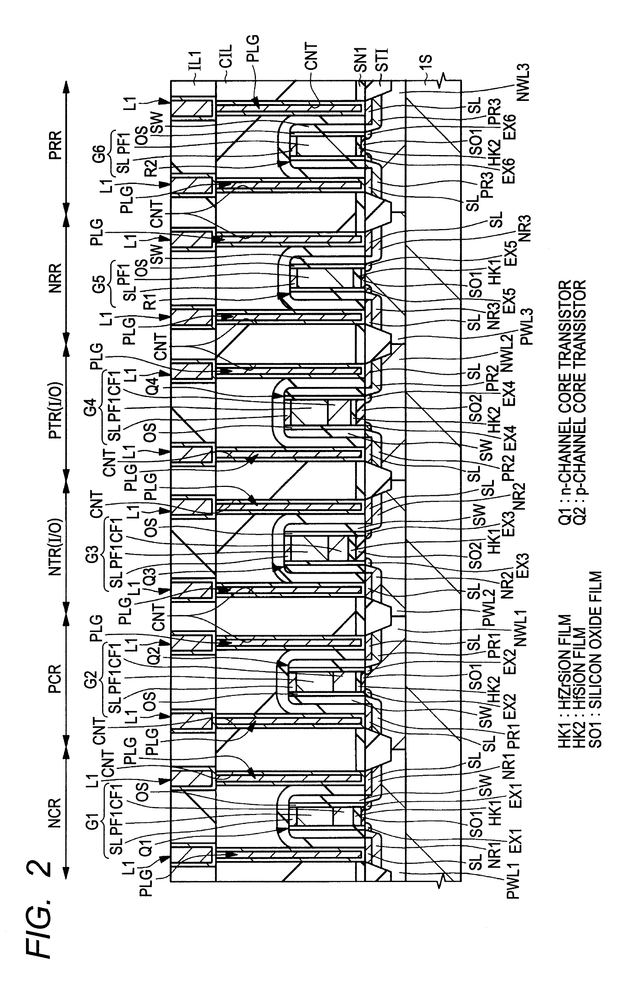
[0185]In the foregoing first embodiment, the description has been given to the example in which, as the gate insulating film of each of the n-channel core transistor Q1, the re-channel I / O transistor Q3, and the n-channel resistor element R1, the HfZrSiON film which is an insulating film containing hafnium and zirconium is used. In the present second embodiment, a description will be given to an example in which, as the gate insulating film of each of the n-channel core transistor Q1, the n-channel I / O transistor Q3, and the re-channel resistor element R1, a HfZrLaSiON film which is an insulating film containing hafnium, zirconium, and lanthanum (La) is used.

[0186]The structure of the semiconductor device in the present second embodiment is substantially the same as in FIG. 2 showing the structure of the semiconductor device in the foregoing first embodiment, and therefore the depiction thereof is omitted. What is different is that, as the gate insulating film of each of the n-chann...

third embodiment

[0194]In the foregoing second embodiment, the description has been given to the example in which, as the gate insulating film of each of the n-channel core transistor Q1, the re-channel I / O transistor Q3, and the n-channel resistor element R1, a HfZrLaSiON film which is an insulating film containing hafnium, zirconium, and lanthanum (La) is used. In the present third embodiment, a description will be given to an example in which, as the gate insulating film of each of the n-channel MISFETs (the n-channel core transistor Q1, the n-channel I / O transistor Q3, and the n-channel resistor element R1), an insulating film containing hafnium, zirconium, and a rare earth element (group III element other than actinium or lanthanoid) is used.

[0195]The structure of the semiconductor device in the present third embodiment is substantially the same as in FIG. 2 showing the structure of the semiconductor device in the foregoing first embodiment, and therefore the depiction thereof is omitted. What ...


PUM


Abstract

There is provided a technology capable of achieving, in a semiconductor device having a MISFET using an insulating film containing hafnium as a gate insulating film, an improvement in the reliability of a MISFET. In the present invention, the gate insulating film of an n-channel core transistor is provided with a structure different from that of the gate insulating film of a p-channel core transistor. Specifically, in the n-channel core transistor, as the gate insulating film thereof, a laminate film of a silicon oxide film and a HfZrSiON film is used. On the other hand, in the p-channel core transistor, as the gate insulating film thereof, a laminate film of a silicon oxide film and a HfSiON film is used.

Description

CROSS-REFERENCE TO RELATED APPLICATIONS[0001]The disclosure of Japanese Patent Application No. 2010-201049 filed on Sep. 8, 2010 including the specification, drawings and abstract is incorporated herein by reference in its entirety.BACKGROUND[0002]The present invention relates to a semiconductor device and a manufacturing technique therefor, and particularly to a technology which is effective when applied to a semiconductor device having a field effect transistor using an insulating film containing hafnium as the gate insulating film and a manufacturing technique therefor.[0003]In Japanese Unexamined Patent Publications Nos. 2009-302260 (Patent Document 1) and 2010-21200 (Patent Document 2), it is described that, for the gate insulating film of a field effect transistor, an oxide of zirconium, an oxynitride thereof, a silicate thereof, or a nitrogen-containing silicate thereof may be used.RELATED ART DOCUMENTSPatent Documents[Patent Document 1][0004]Japanese Unexamined Patent Public...

Claims


Application Information

Patent Timeline
IPC IPC(8): H01L21/8238H01L27/092
CPCH01L21/823857H01L27/105H01L29/7833H01L29/517H01L29/518H01L28/20
Inventor MIZUTANI, MASAHARUKADOSHIMA, MASARUKAWAHARA, TAKAAKIINOUE, MASAOUMEDA, HIROSHI
Owner RENESAS ELECTRONICS CORP
Why Eureka
Try Eureka