Method and System for Forming High Accuracy Patterns Using Charged Particle Beam Lithography

a technology of charged particle beam and pattern, applied in the field of lithography, can solve the problems of high computational cost, difficult to accurately translate the physical design to the actual circuit pattern developed on the resist layer, and difficult to add opc features, etc., to improve critical dimension variation and line-edge roughness, improve the effect of dose margin and improve the accuracy of lithography

Active Publication Date: 2012-04-19
D2S
View PDF3 Cites 26 Cited by
  • Summary
  • Abstract
  • Description
  • Claims
  • Application Information

AI Technical Summary

Benefits of technology

[0016]A method and system for fracturing or mask data preparation for charged particle beam lithography are disclosed in which accuracy and/or dose margin of a pattern formed on a surface by a set of charged particle beam shots is enhanced by use of partially-overlapping shots. In some embodiments, dosage

Problems solved by technology

An example of an end-use limitation is defining the geometry of a transistor in a way in which it cannot sufficiently operate at the required supply voltage.
The design rule limitations reflect, among other things, the smallest dimensions that can be reliably fabricated.
As the critical dimensions of the circuit pattern become smaller and approach the resolution value of the exposure tool, the accurate transcription of the physical design to the actual circuit pattern developed on the resist layer becomes difficult.
Adding OPC features is a very laborious task, requires costly computation time, and results in more expensive reticles.
Not only are OPC patterns complex, but since optical proximity effects are long range compared to minimum line and space dimensions, the correct OPC patterns in a given location depend significantly on what other geometry is in the neighborhood.
There are numerous manufacturing factors that also cause variations, but the OPC component of that overall error is often in the range listed.
Since curvilinear patterns are difficult and expensive to form on a reticle using conventional techniques, rec

Method used


Image

  • Method and System for Forming High Accuracy Patterns Using Charged Particle Beam Lithography
  • Method and System for Forming High Accuracy Patterns Using Charged Particle Beam Lithography
  • Method and System for Forming High Accuracy Patterns Using Charged Particle Beam Lithography

Examples


Embodiment Construction

[0035]The present disclosure describes a method for enhancing the accuracy of charged particle beam exposure by use of overlapping shots. The present invention enhances the ability of charged particle beam systems to accurately produce patterns smaller than 100 nm on a reticle, with acceptable CD variation and LER in light of manufacturing variation. Additionally, the present invention expands the process window of manufacturing variations under which these accurate patterns may be produced.

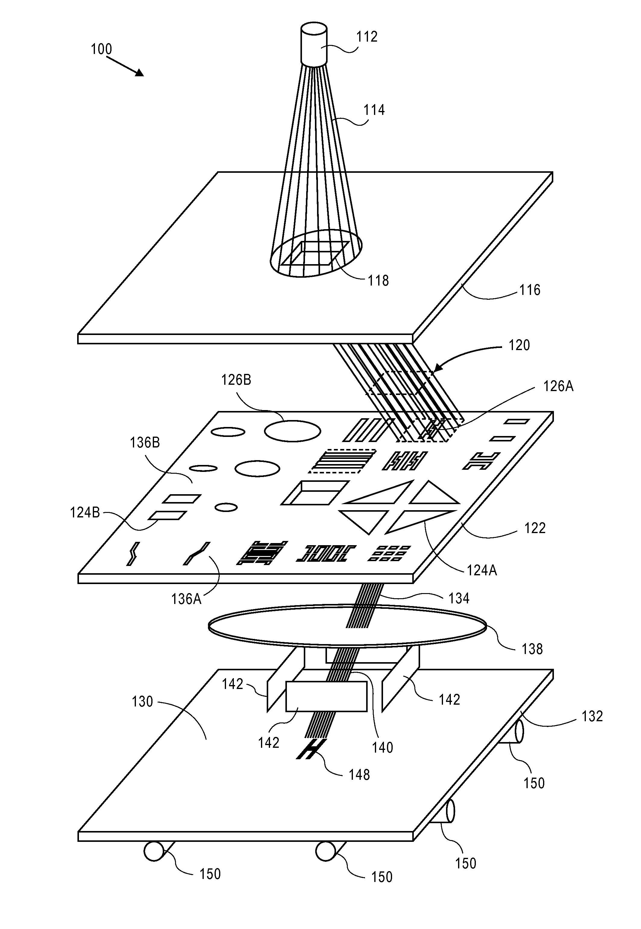
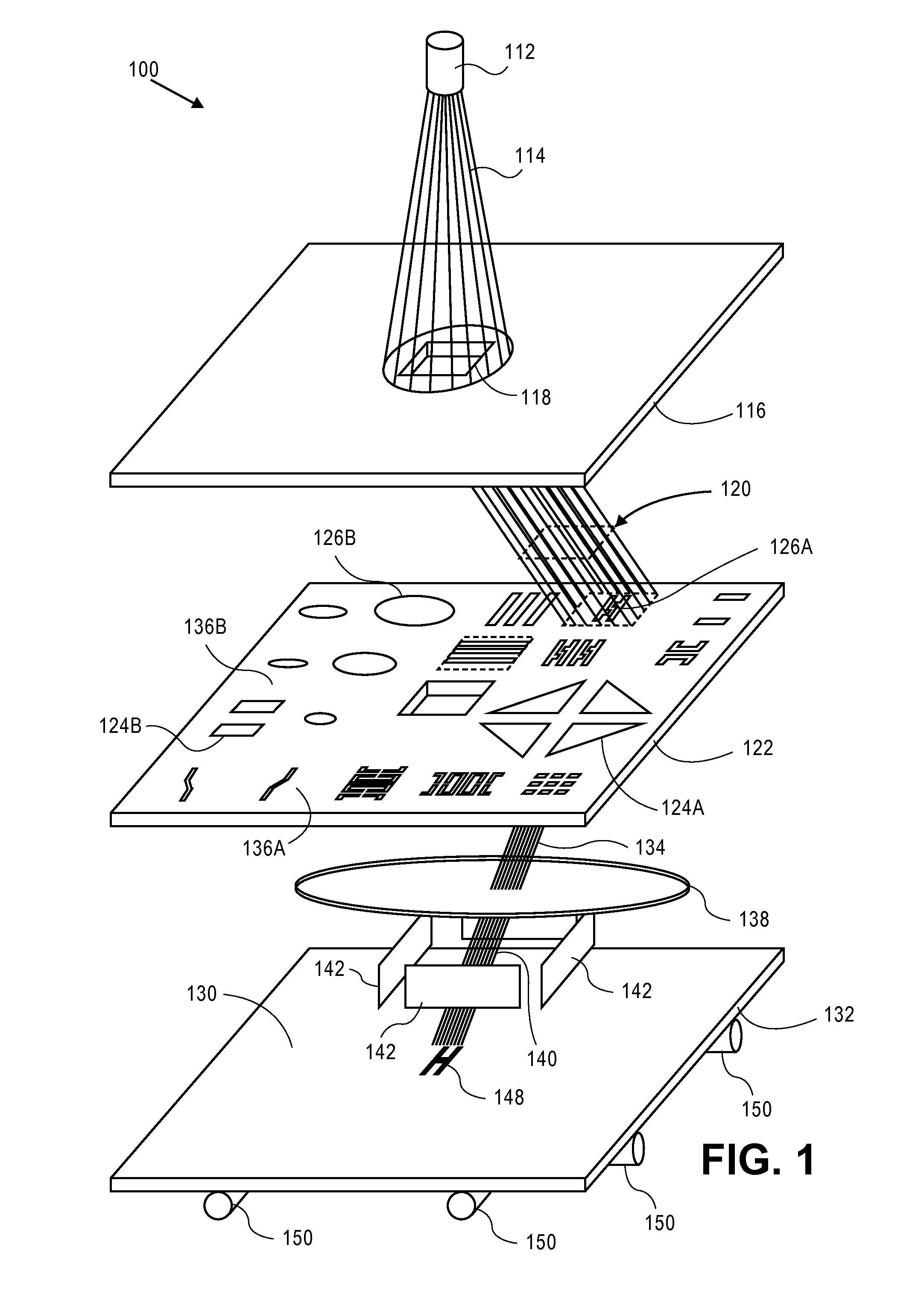
[0036]Referring now to the drawings, wherein like numbers refer to like items, FIG. 1 illustrates an embodiment of a conventional lithography system 100, such as a charged particle beam writer system, in this case an electron beam writer system, that employs character projection to manufacture a surface 130. The electron beam writer system 100 has an electron beam source 112 that projects an electron beam 114 toward an aperture plate 116. The plate 116 has an aperture 118 formed therein which all...


PUM


Abstract

A method and system for fracturing or mask data preparation for charged particle beam lithography are disclosed in which accuracy and/or edge slope of a pattern formed on a surface by a set of charged particle beam shots is enhanced by use of partially-overlapping shots. In some embodiments, dosages of the shots may vary with respect to each other before proximity effect correction. Particle beam simulation may be used to calculate the pattern and the edge slope. Enhanced edge slope can improve critical dimension (CD) variation and line-edge roughness (LER) of the pattern produced on the surface.

Description

RELATED APPLICATIONS[0001]This application: 1) claims priority to U.S. Provisional Patent Application Ser. No. 61 / 392,477 filed on Oct. 13, 2010 and entitled “Method for Integrated Circuit Manufacturing and Mask Data Preparation Using Curvilinear Patterns”; and 2) is related to Fujimura, U.S. patent application Ser. No. ______, entitled “Method and System for Forming Patterns with Charged Particle Beam Lithography” (Attorney Docket No. D2SiP038) filed on even date herewith; both of which are hereby incorporated by reference for all purposes.BACKGROUND OF THE DISCLOSURE[0002]The present disclosure is related to lithography, and more particularly to the design and manufacture of a surface which may be a reticle, a wafer, or any other surface, using charged particle beam lithography.[0003]In the production or manufacturing of semiconductor devices, such as integrated circuits, optical lithography may be used to fabricate the semiconductor devices. Optical lithography is a printing proc...

Claims


Application Information

Patent Timeline
IPC IPC(8): G06F17/50
CPCG06F17/5077G06F2217/12G06F17/5081G03F7/70441G06F30/394G06F30/398G06F2119/18
Inventor FUJIMURA, AKIRAHAGIWARA, KAZUYUKIMEIER, STEPHEN F.BORK, INGO
Owner D2S
Why Eureka
Try Eureka