Semiconductor device having stacked array structure, NAND flash memory array using the same and fabrication thereof

a technology of stacked array and semiconductor devices, which is applied in the direction of memory adressing/allocation/relocation, semiconductor devices, instruments, etc., can solve the problems limitation of high integration of nand flash memory arrays, and limitation of high integration of memory arrays, so as to improve controllability of channels, improve cell operation properties, and widen channel width

Active Publication Date: 2012-05-10
SEOUL NAT UNIV R&DB FOUND
View PDF1 Cites 17 Cited by
  • Summary
  • Abstract
  • Description
  • Claims
  • Application Information

AI Technical Summary

Benefits of technology

[0019]According to the configuration of a semiconductor device having the STAR structure, the present invention has an advantageous effect of vertically forming a plurality of semiconductor devices enabling to widen the width of a channel by having a vertical channel region and forming source/drain regions on left and right sides of the channel region and to have one of single gate (SG), double gate (DG) and gate all around (GAA) structures passing by to cross or wrap around one or more of the vertically stacked semiconductor layers and sharing a body with adjacent devices to have a body contact as occasion demands.
[0020]Specifically, when the semiconductor device according to the present invention has the gate all around (GAA) structure to wrap around each of the semiconductor layers by one gate electrode for forming a cube or cylinder shaped channel by the cross-sectional shape of each of the semiconductor layers, it is possible to greatly improve controllability to a channel by the gate electrode.
[0021]Furthermore, when the semiconductor device with the GAA structure is used as a memory cell, the operation properties of the cell are also greatly improved by a single or multilayer insulator with various radii of curvature interlaid between the gate electrode and each of the semiconductor layers.
[0022]A NAND flash memory array using the semiconductor device having the STAR structure as a memory cell according to the present in

Problems solved by technology

Currently, most MOSFETs used as a switch device have a planar type structure which takes up a lot of space to make a switch device of a memory array such as a 1T-DRAM etc. and there has been a limitation on a high integration of the memory array.
Also, most memory devices used as a memory cell have a planar type structure and have the above mentioned problem.
But there has been a limitation on the high integration of the memory array by using a planar type memory cell.
However, so far, because t

Method used


Image

  • Semiconductor device having stacked array structure, NAND flash memory array using the same and fabrication thereof
  • Semiconductor device having stacked array structure, NAND flash memory array using the same and fabrication thereof
  • Semiconductor device having stacked array structure, NAND flash memory array using the same and fabrication thereof

Examples


embodiment 1

[Embodiment 1 on Method for Fabricating NAND Flash Memory Array]

[0064]For embodiments of a method for fabricating a NAND flash memory array having a STAR structure according to the present invention, first methods for fabricating bit lines and word lines required commonly are described with respect to FIGS. 10 to 20 as follows:

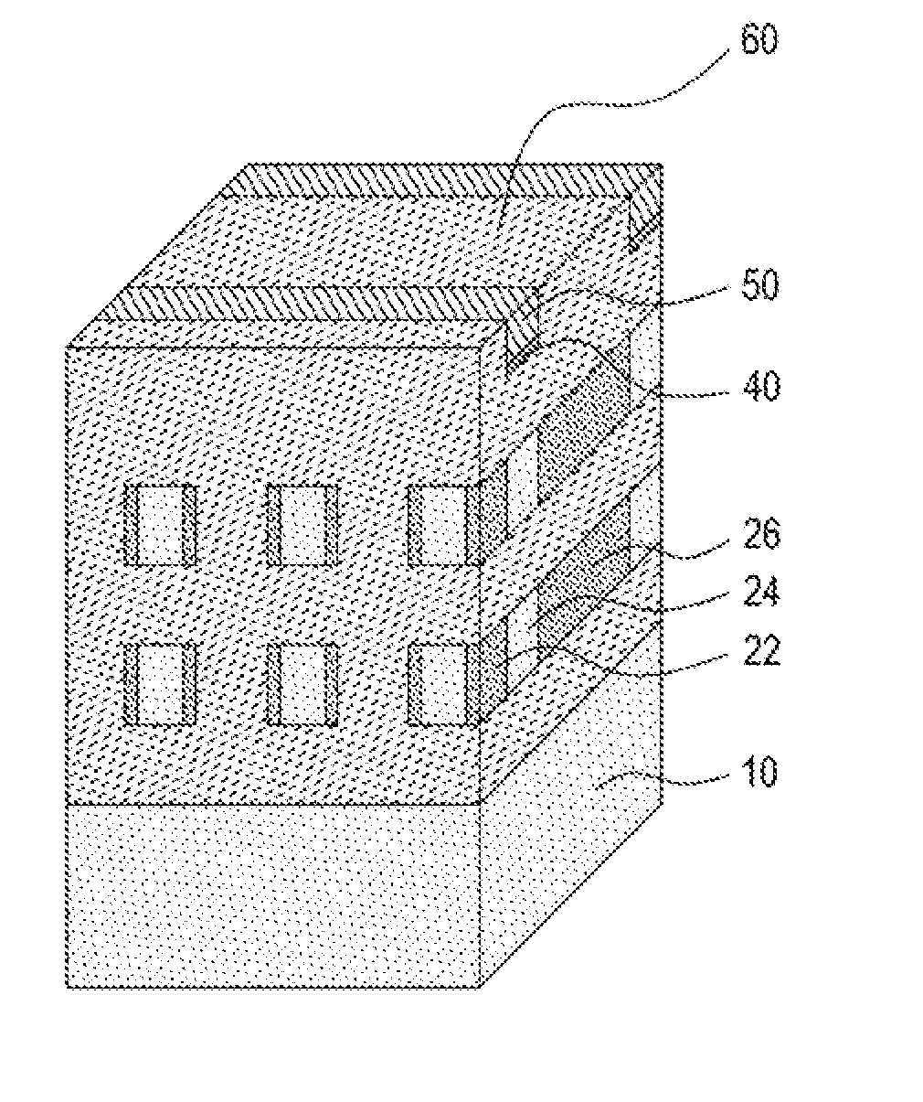
[0065]First, as shown in FIG. 10, “a semiconductor layer 220 on a stack mediate layer 210” is formed iteratively n times (for convenience, FIG. 10 shows only 2 times repeated formation) on a predetermined substrate 100, an n+1th stack mediate layer (in FIG. 10, 3rd stack mediate layer 250) is formed on the nth semiconductor layer (in FIG. 10, 2nd semiconductor layer 240), and a first etching mask 330 is formed on the n+1th stack mediate layer 250 (step 1).

[0066]Here, the stack mediate layers 210, 230 and 250 and the semiconductor layers 220 and 240 are preferably stacked by the epitaxial method for growing a single crystal.

[0067]The stack mediate layers 210, 2...

embodiment 2

[Embodiment 2 on Method for Fabricating NAND Flash Memory Array]

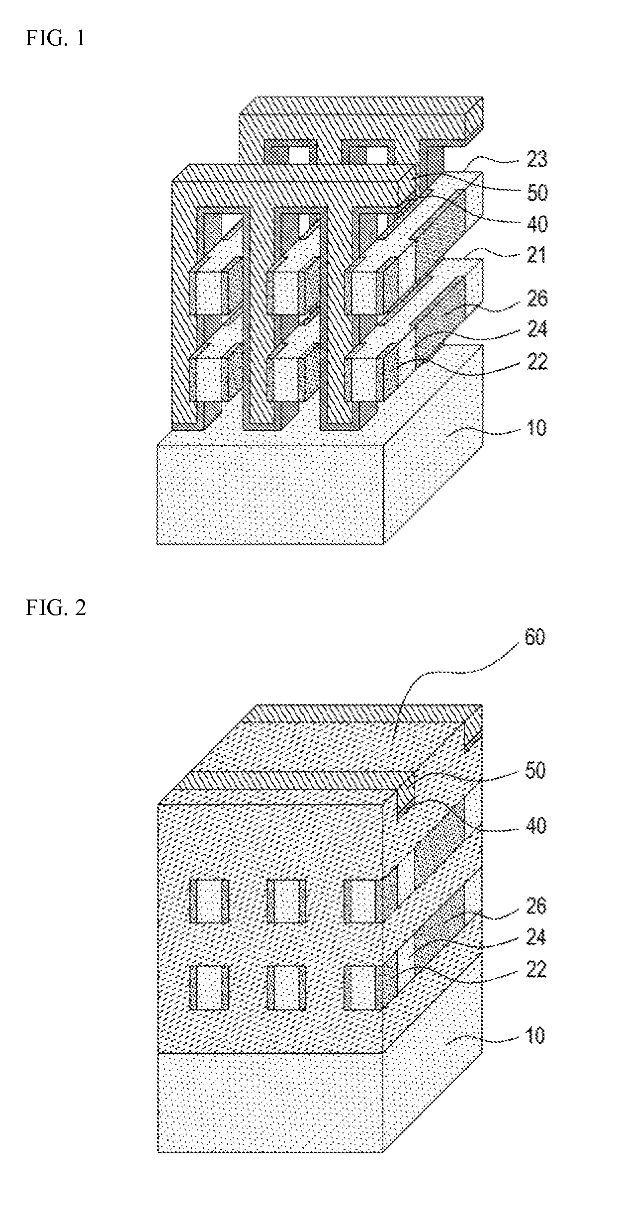
[0098]This embodiment is performed as like as Embodiment 1 but, between steps 5 and 6, a curving process is further added to curve the surfaces of the semiconductor layers, as reference numbers 220b and 240b shown in FIG. 16, exposed at both sides of the partitions 712 and 722.

[0099]By the curving process, the further processes are proceeded as follows: forming cylindrical insulator layers 420 on the cylindrical semiconductor layers 220b and 240b (as shown in FIG. 17), forming the word lines 500 by depositing a gate material to wrap around the cylindrical insulator layers 420 between the partitions 712 and 722 (as shown in FIG. 18), removing the partitions 712 and 722 and then filling the empty spaces with the interlayer insulator 600 (when the source / drain regions of cell are formed by fringing fields) or forming the impurity-doped layers to form the source / drain regions 224 and 226 on each of the semiconductor layers ...

embodiment 3

[Embodiment 3 on Method for Fabricating NAND Flash Memory Array]

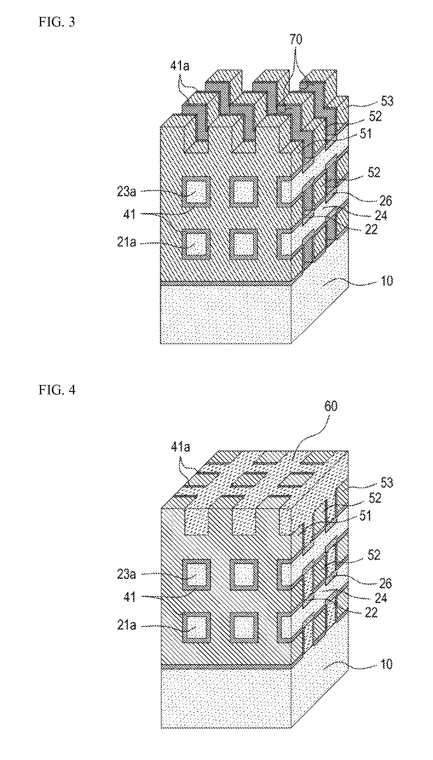
[0103]This embodiment relates mainly to a fabricating method for formation of impurity-doped layers for short circuit and of bit select lines. This embodiment comprises a fabricating method according to Embodiment 1 or 2 and additional processes as the following: forming a short-circuit impurity-doped layer 222 or 242 in the semiconductor layer exposed by the opening of a doping mask 310 or 320 formed to have a different opening site per formation of “semiconductor layer on stack mediate layer” in step 1 as shown in FIGS. 8 and 9, and simultaneously forming bit select lines BSL1 and BSL2 as many as the number (n) of the stacked semiconductor layers to pass by the short-circuit impurity-doped layers 222 and 242 at forming the word lines in step 7.

[0104]In other words, as shown in FIG. 7, after formation of the “semiconductor layer 220 / stack mediate layer 210” on the substrate 100, as shown in FIG. 8, a first doping mask ...


PUM


Abstract

The present invention relates to a semiconductor device, a memory array and a fabrication method thereof, and more particularly to a semiconductor device having a stacked array structure (referred to as a STAR structure: a STacked ARray structure) applicable to not only a switch device but also a memory device, a NAND flash memory array using the same as a memory device and a fabrication method thereof.

Description

BACKGROUND OF THE INVENTION[0001]1. Field of the Invention[0002]The present invention relates to a semiconductor device, a memory array and a fabrication method thereof, and more particularly to a semiconductor device having a stacked array structure (hereinafter referred to as a STAR structure: a STacked ARray structure) applicable to not only a switch device but also a memory device, a NAND flash memory array using the same as a memory device and a fabrication method thereof.[0003]2. Description of the Related Art[0004]Currently, most MOSFETs used as a switch device have a planar type structure which takes up a lot of space to make a switch device of a memory array such as a 1T-DRAM etc. and there has been a limitation on a high integration of the memory array.[0005]Also, most memory devices used as a memory cell have a planar type structure and have the above mentioned problem.[0006]Particularly, since the high integration of a NAND flash memory array is easier than that of a NOR...

Claims


Application Information

Patent Timeline
IPC IPC(8): G06F12/02
CPCH01L27/115H01L27/11521H01L27/11582H01L27/11578H01L27/11565H10B69/00H10B41/30H10B43/10H10B43/20H10B43/27H10B63/80
Inventor PARK, BYUNG GOOKYUN, JANG GNPARK, IL HAN
Owner SEOUL NAT UNIV R&DB FOUND
Why Eureka
Try Eureka