Semiconductor circuit, method for driving the same, storage device, register circuit, display device, and electronic device

Active Publication Date: 2012-06-28
SEMICON ENERGY LAB CO LTD
View PDF6 Cites 54 Cited by
  • Summary
  • Abstract
  • Description
  • Claims
  • Application Information

AI Technical Summary

Benefits of technology

[0028]By application of a semiconductor device of the present invention to a storage device such as a register circuit, it is possible to obtain a storage device in which data can be retained even when supply of power is interrupted, refresh (reset) operation can be performed, and power consumption is markedly reduced. By application of such a storage device to an arithmetic unit such as a CPU, an electronic device such as a personal computer or a cellular phone that includes the arithmetic unit can be an electronic device in which supply of power can be temporarily interrupted, power consumption is low, and restart operation is performed quickly.
[0029]By application of the semiconductor device of the present invention to

Problems solved by technology

The threshold voltage of a transistor easily fluctuates depending on steps of manufacturing the transistor, and it is difficult to control the threshold voltage of the tra

Method used


Image

  • Semiconductor circuit, method for driving the same, storage device, register circuit, display device, and electronic device
  • Semiconductor circuit, method for driving the same, storage device, register circuit, display device, and electronic device
  • Semiconductor circuit, method for driving the same, storage device, register circuit, display device, and electronic device

Examples


Example

Embodiment 1

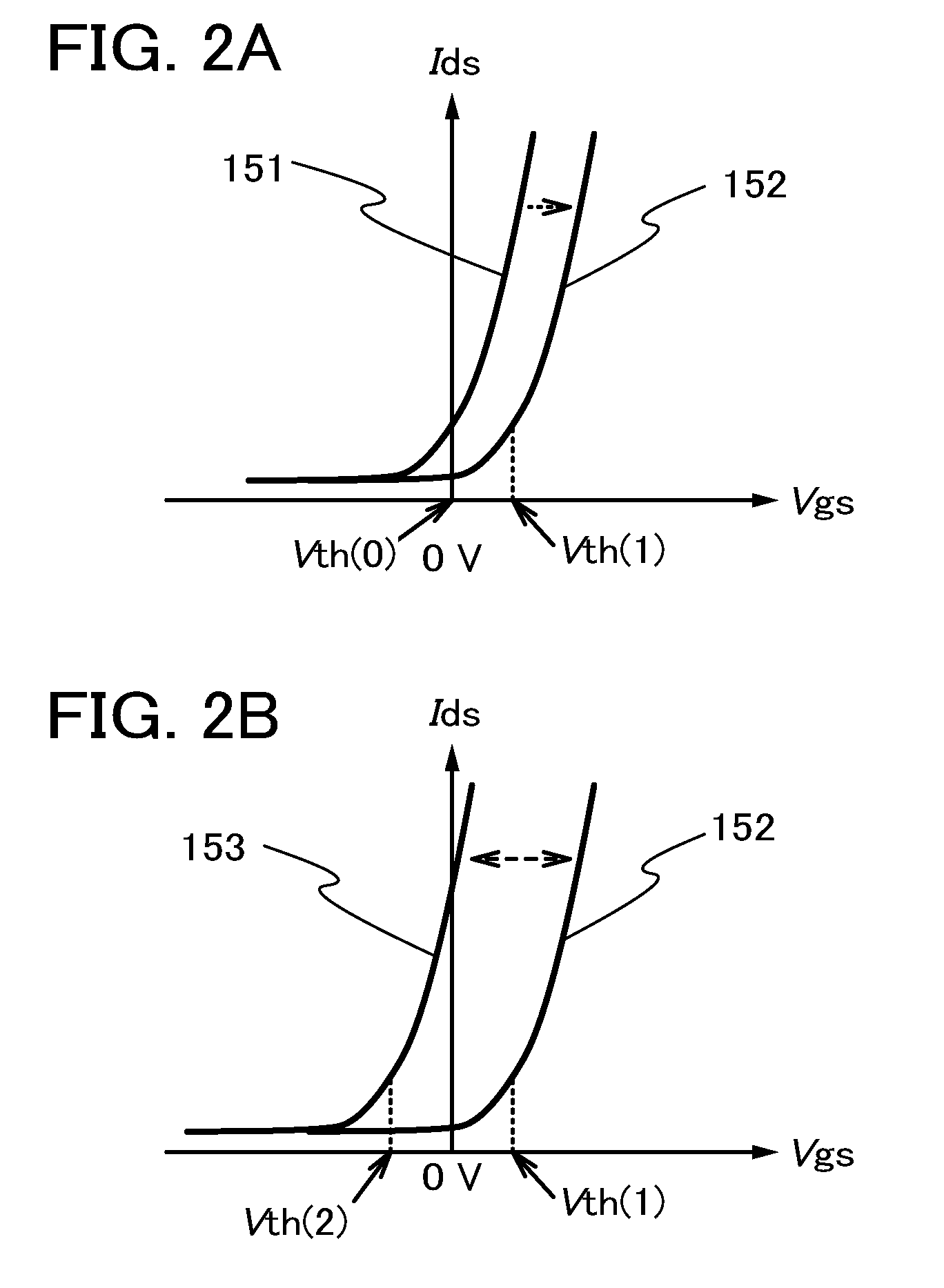
[0051]In this embodiment, examples of a semiconductor circuit capable of controlling the threshold voltage of a transistor in the present invention are described with reference to FIGS. 1A and 1B, FIGS. 2A and 2B, and FIGS. 3A and 3B.

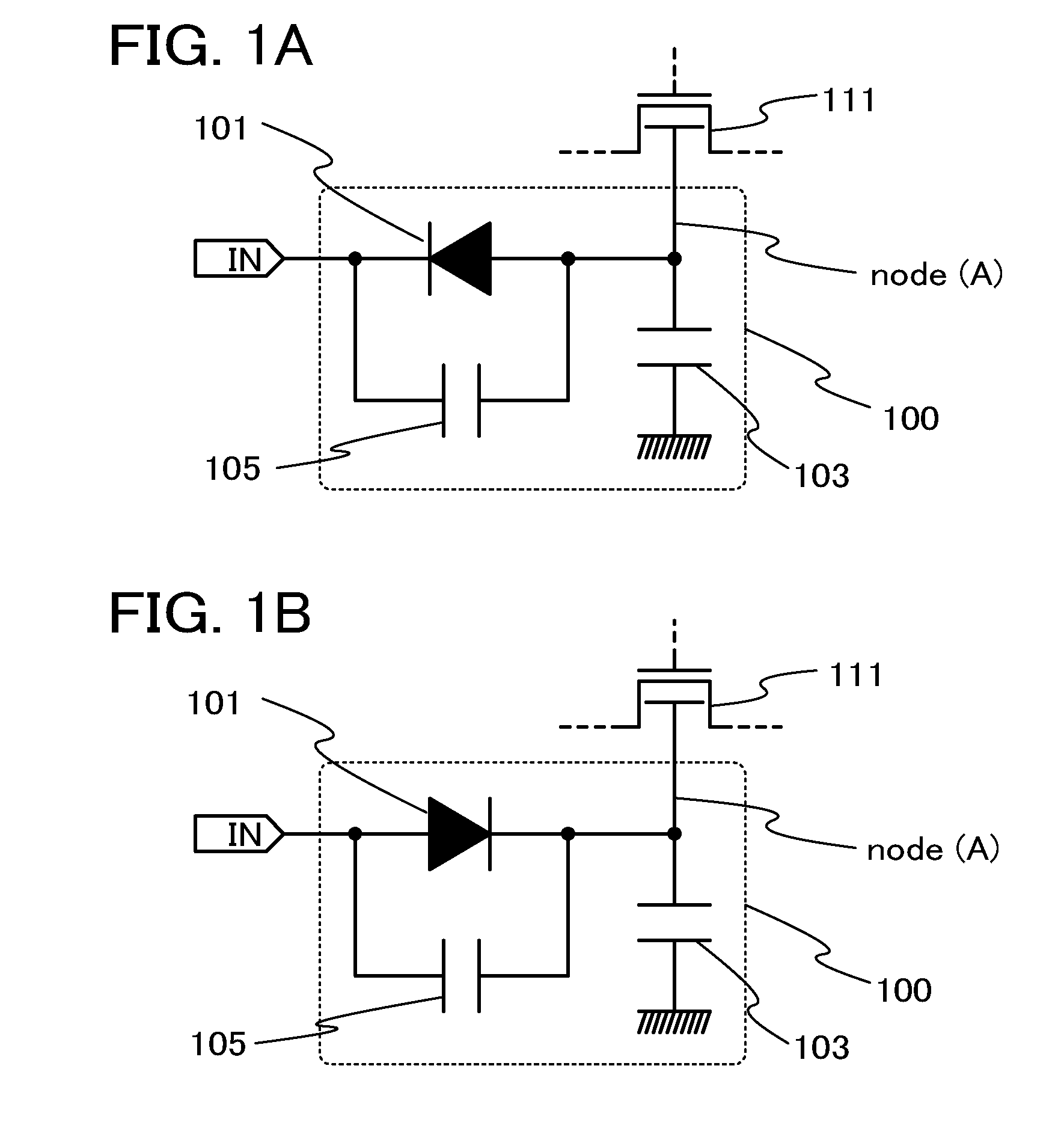
[0052]FIG. 1A illustrates a control circuit 100 in this embodiment and a transistor 111 connected to the control circuit 100.

[0053]The transistor 111 includes a back gate (a second gate electrode), and output voltage from the control circuit 100 is input to the back gate. Although an n-channel transistor is used as the transistor 111 in this embodiment, a p-channel transistor can be used.

[0054]The control circuit 100 includes a diode 101, a capacitor 103, and a capacitor 105. An input terminal IN is connected to the control circuit 100. A second electrode of the diode 101 is connected to an input portion, and a first electrode of the diode 101 is connected to a first electrode of the capacitor 103. A second electrode of the capacitor 103 is ...

Example

Embodiment 2

[0077]In this embodiment, a structure example where the semiconductor circuit capable of controlling the threshold voltage of a transistor in Embodiment 1 is used as a register circuit that is one of storage devices is described with reference to FIGS. 4A and 4B.

[0078]FIG. 4A illustrates a structure example of a 1-bit register circuit to which the control circuit 100 in Embodiment 1 is connected. A register circuit 200 includes a transistor 201, a capacitor 203, and a flip-flop circuit 205. In this embodiment, an n-channel transistor is used as the transistor 201.

[0079]The transistor 201 includes a back gate (a second gate electrode) as in the transistor 111 in Embodiment 1, and output voltage from the control circuit 100 is input to the back gate. An input terminal Sig1 is connected to a first gate electrode of the transistor 201, an input terminal Sig2 is connected to a first electrode of the transistor 201, and the transistor 201 is controlled with input signals from ...

Example

Embodiment 3

[0105]In this embodiment, an example where the semiconductor circuit capable of controlling the threshold voltage of a transistor in Embodiment 1 is used as a storage device whose structure is different from the structure of the storage device in Embodiment 2 is described with reference to FIGS. 5A and 5B.

[0106]FIG. 5A illustrates a structure example of a 1-bit memory cell 250 to which the control circuit 100 in Embodiment 1 is connected. The memory cell 250 includes a transistor 251, a capacitor 253, and a transistor 255. In this embodiment, an n-channel transistor is used as the transistor 251 as in the transistor 201 in Embodiment 2.

[0107]Output voltage from the control circuit 100 is input to a back gate of the transistor 251. An input terminal Sig3 is connected to a first gate electrode of the transistor 251, an input terminal Sig4 is connected to a first electrode of the transistor 251, and the transistor 251 is controlled with control signals from the two input te...


PUM


Abstract

A semiconductor circuit capable of controlling and holding the threshold voltage of a transistor at an optimal level and a driving method thereof are disclosed. A storage device, a display device, or an electronic device including the semiconductor circuit is also provided. The semiconductor circuit comprises a diode and a first capacitor provided in a node to which a transistor to be controlled is connected through its back gate. This structure allows the application of desired voltage to the back gate so that the threshold voltage of the transistor is controlled at an optimal level and can be held for a long time. A second capacitor connected in parallel with the diode is optionally provided so that the voltage of the node can be changed temporarily.

Description

BACKGROUND OF THE INVENTION[0001]1. Field of the Invention[0002]The present invention relates to semiconductor circuits and methods for driving the semiconductor circuits. The present invention relates to storage devices, display devices, and electronic devices.[0003]2. Description of the Related Art[0004]A field-effect transistor (FET) (hereinafter also referred to as a transistor) has three electrodes: a source, a gate, and a drain, and controls the flow of electrons or holes between the source and the drain by application of voltage to the gate. As a semiconductor used for an active layer, a Group IV element such as silicon or germanium, a Group III-V compound such as gallium arsenide, indium phosphide, or gallium nitride, a Group II-VI compound such as zinc sulfide or cadmium telluride, or the like can be used.[0005]In recent years, FETs including an oxide such as zinc oxide or an indium gallium zinc oxide-based compound as a semiconductor have been reported (References 1 and 2)...

Claims


Application Information

Patent Timeline
IPC IPC(8): H01L29/786H01L33/16
CPCG09G3/3648G09G2300/043H01L27/1225G09G2320/0214G09G2300/0819H01L28/40H01L27/1214H01L29/78606H01L29/78618H01L29/7869H01L29/78696H01L27/1255
Inventor ENDO, MASAMIOHSHIMA, KAZUAKI
Owner SEMICON ENERGY LAB CO LTD
Why Eureka
Try Eureka