Area array semiconductor device package interconnect structure with optional package-to-package or flexible circuit to package connection

Active Publication Date: 2012-06-28
HSIO TECH
View PDF4 Cites 55 Cited by
  • Summary
  • Abstract
  • Description
  • Claims
  • Application Information

AI Technical Summary

Benefits of technology

[0022]The present IC package can be produced digitally, without tooling or costly artwork. The high performance electrical interconnect can be produced as a “Green” product, with dramatic reductions in environmental issues related to the production of conventional flexible circuits.
[0023]The use of additive printing processes permits the material set in a given layer to vary. Traditional PCB and flex circuit fabrication methods take sheets of material and stack them up, laminate, and/or drill. The materials in each layer are limite

Problems solved by technology

In many cases, the size and distance between die terminals is so small that the device cannot be connected to the final PCB without some sort of fan out or routing.
In many cases, the size and distance between die terminals is so small that the IC device cannot be connected to the final PCB without some sort of re-routing interface.
In both cases, the connection of the device to the package is generally not reworkable once packaged and if there is a missing or broken connection it is difficult to repair.
In many cases, the functional performance of the device is not known prior

Method used


Image

  • Area array semiconductor device package interconnect structure with optional package-to-package or flexible circuit to package connection
  • Area array semiconductor device package interconnect structure with optional package-to-package or flexible circuit to package connection
  • Area array semiconductor device package interconnect structure with optional package-to-package or flexible circuit to package connection

Examples


Embodiment Construction

[0062]A high performance IC package according to the present disclosure may permit fine contact-to-contact spacing (pitch) on the order of less than 1.0 mm pitch, and more preferably a pitch of less than about 0.7 millimeter, and most preferably a pitch of less than about 0.4 millimeter. Such fine pitch high performance IC packages are especially useful for communications, wireless, and memory devices.

[0063]The present IC package can be configured as a low cost, high signal performance electrical interconnect, which has a low profile that is particularly useful for desktop and mobile PC applications. IC devices can be installed and uninstalled without the need to reflow solder. The solder-free electrical connection of the IC devices is environmentally friendly.

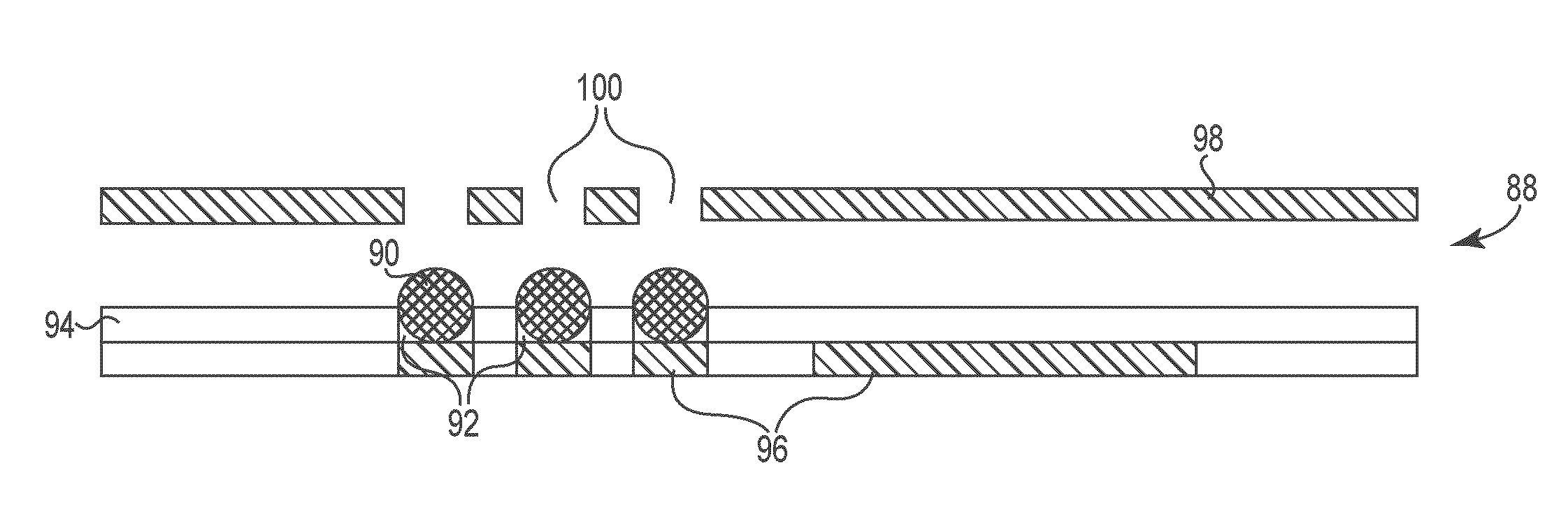
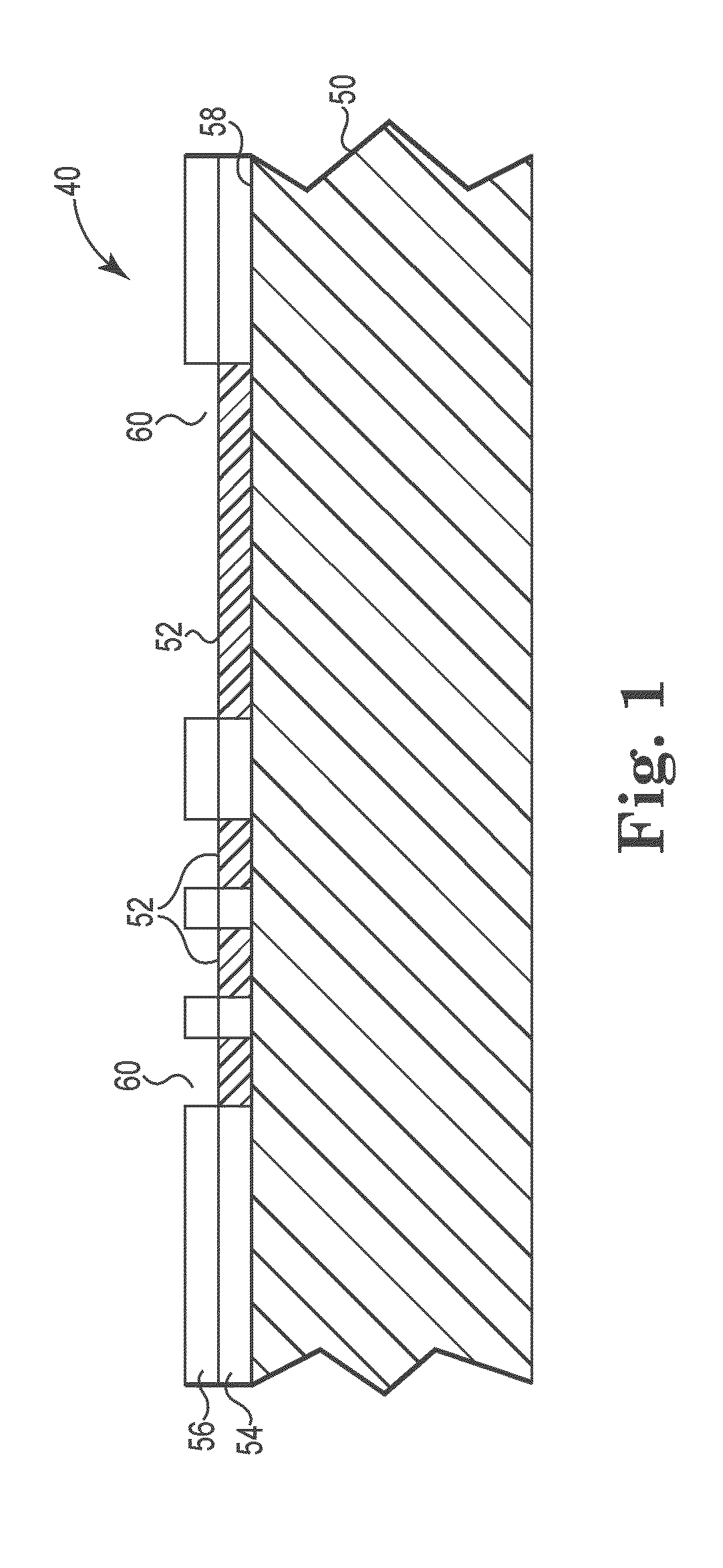
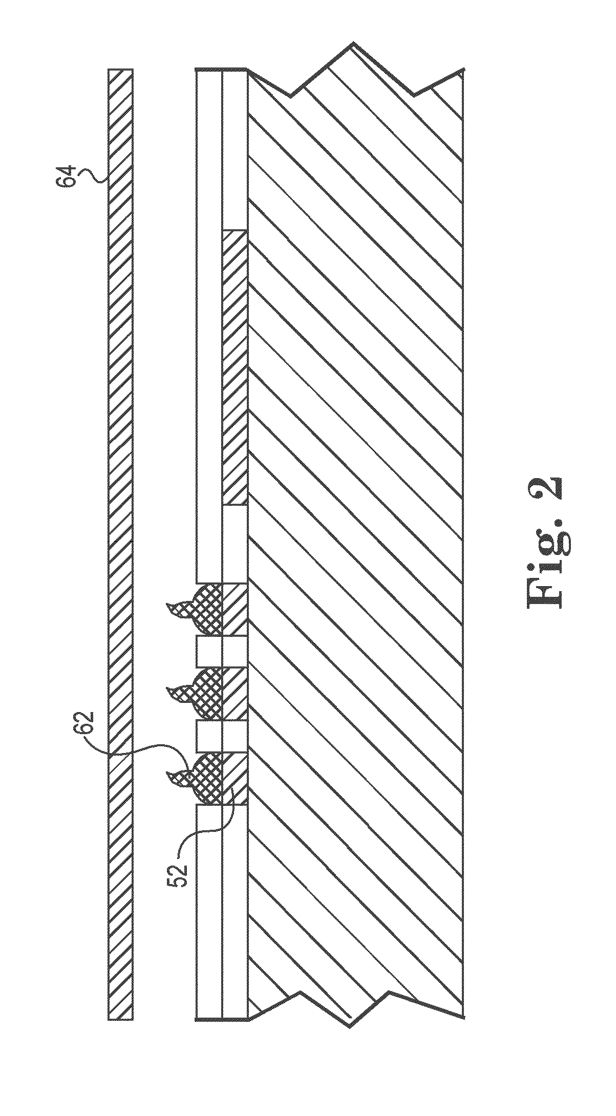
[0064]FIG. 1 is a side cross-sectional view of a method of making an electrical interconnect 40 using additive processes for use in an IC package in accordance with an embodiment of the present disclosure. The process starts s...


PUM


Abstract

An area array integrated circuit (IC) package for an IC device. The IC package includes a first substrate with conductive traces electrically coupled to the IC device. An interconnect assembly having a first surface is mechanically coupled to the first substrate. The interconnect assembly includes a plurality of contact members electrically coupled to the conductive traces on the first substrate. A second substrate is mechanically coupled to a second surface of the interconnect assembly so that the first substrate, the interconnect assembly, and the second substrate substantially surround the IC device. The second substrate includes conductive traces that are electrically coupled to the contact members in the interconnect assembly.

Description

[0001]This application claims the benefit of U.S. Provisional Application No. 61 / 448,282, filed Mar. 2, 2011, the disclosure of which is hereby incorporated by reference.[0002]This application is a continuation-in-part of U.S. patent application Ser. No. 13 / 266,573, titled COMPLIANT PRINTED CIRCUIT AREA ARRAY SEMICONDUCTOR DEVICE PACKAGE, filed Oct. 27, 2011, which is a national stage application under 35 U.S.C.§371 of International Application No. PCT / US2010 / 036363, titled COMPLIANT PRINTED CIRCUIT AREA ARRAY SEMICONDUCTOR DEVICE PACKAGE, filed May 27, 2010, which claims priority to U.S. Provisional Application No. 61 / 183,411, filed Jun. 2, 2009, all of which are hereby incorporated by reference in their entireties.[0003]This application is a continuation-in-part of U.S. patent application Ser. No. 13 / 318,200, title COMPLIANT PRINTED CIRCUIT WAFER LEVEL SEMICONDUCTOR PACKAGE, filed Oct. 31, 2011, which is a national stage application under 35 U.S.C.§371 of International Application...

Claims


Application Information

Patent Timeline
IPC IPC(8): H01L23/48H01L21/60
CPCH01L21/6835H01L2924/15311H01L24/13H01L24/16H01L24/81H01L2221/68345H01L2224/16225H01L2224/81005H01L2224/81201H01L2224/8138H01L2224/819H01L2924/09701H05K3/3436H01L2924/01087H01L23/49811H01L23/49822H01L23/49827H01L23/49838H01L2224/81191H01L23/60H01L2924/14H01L2224/131H01L2924/00H01L2924/014H01L2924/00014
Inventor RATHBURN, JAMES
Owner HSIO TECH
Why Eureka
Try Eureka