

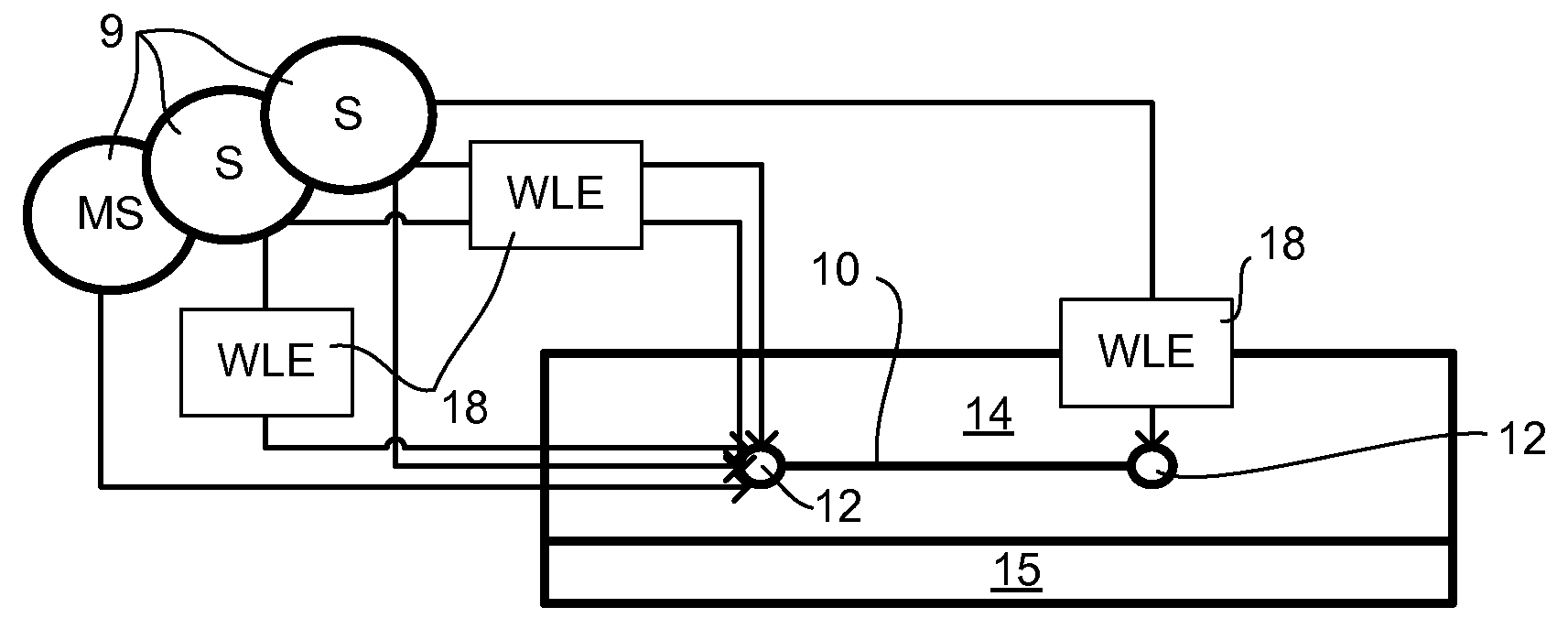
Composite subwavelength-structured waveguide in optical systems
a subwavelength structure and optical system technology, applied in the field of waveguides, can solve the problems of miniaturization of this type of waveguide, light scattering loss, and limited desired waveguide properties, and achieve the effects of effective cancelling dispersion, thermal dependence or other propagation characteristics, and reducing the number of optical waveguides
- Summary
- Abstract
- Description
- Claims
- Application Information
AI Technical Summary
Benefits of technology
Problems solved by technology
Method used
Image

Examples
examples
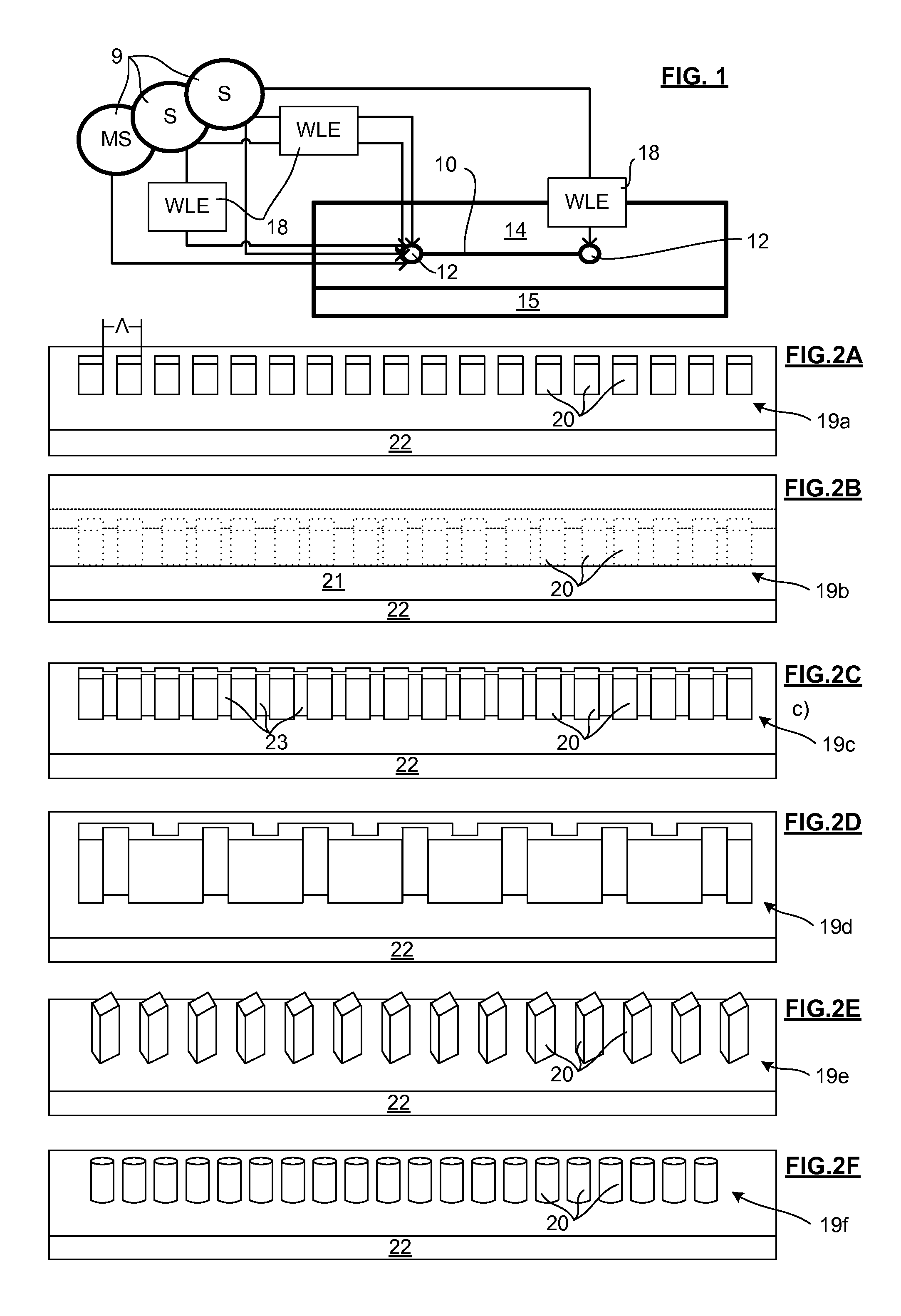
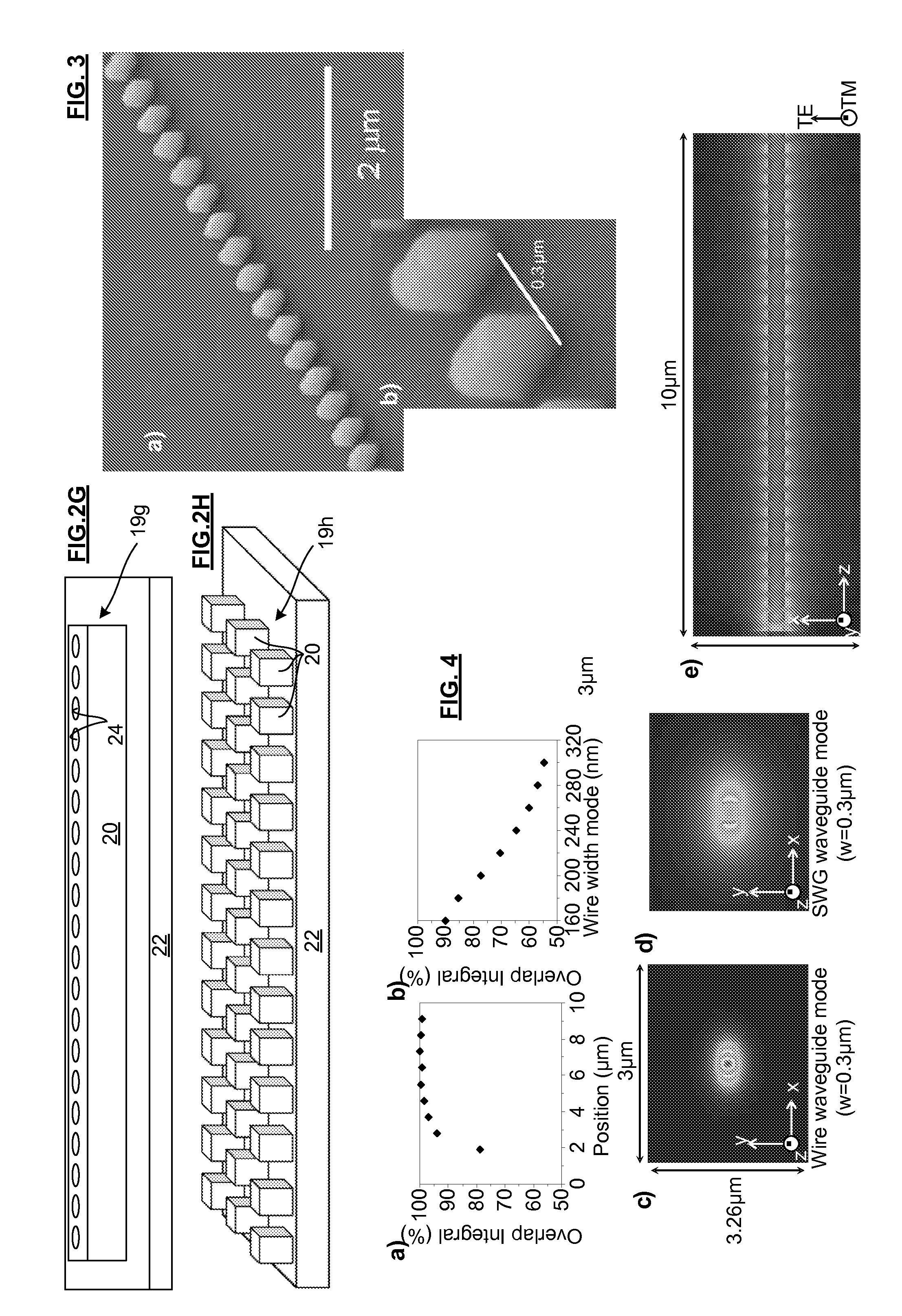
[0064]Applicant has demonstrated SWG waveguides on silicon. Silicon is a preferred waveguide material in the near-infrared due to its high dielectric permittivity, which allows compact photonic circuits to be made, with the added advantage of leveraging the vast manufacturing infrastructure developed by the silicon microelectronics industry. SWG is a relatively easy to produce composite subwavelength-structure. A typical SWG silicon waveguide core (prior to SU8 in-fill) of our experiments is shown in FIGS. 3a,b. The waveguide core was a linear periodic array of rectangular segments etched from a 260-nm-thick single crystal silicon layer of a silicon-on-insulator (SOI) wafer. A 2-μm thick bottom oxide (SiO2) layer separates the waveguide from the underlying silicon substrate, to form a bottom cladding. The nominal structural period of the SWG was d=300 nm, which is less than a half of the effective wavelength of the waveguide mode λeff (λeff=λ / neff) for which the waveguide was design...
PUM
| Property | Measurement | Unit |
|---|---|---|
| size | aaaaa | aaaaa |
| wavelengths | aaaaa | aaaaa |
| wavelengths | aaaaa | aaaaa |
Abstract
Description
Claims
Application Information