Fabrication of Microfilters and Nanofilters and Their Applications

a technology of nanofilters and microfilters, applied in water/sewage treatment, osmosis/dialysis, photographic processes, etc., can solve the problems of large holes, fragile samples requiring structural support, and inability to meet the needs of use,

Active Publication Date: 2012-07-19
CREATV MICROTECH
View PDF16 Cites 47 Cited by
  • Summary
  • Abstract
  • Description
  • Claims
  • Application Information

AI Technical Summary

Problems solved by technology

Although this technique offers the advantage of submicron resolution over large sample areas and through the entire resist thickness, most papers on this subject report aspect ratios below 2, which results in thin, fragile samples requiring structural support often provided by silicon frames.
The pores are located randomly and they often overlap resulting in large holes.
For some applications, it is not a desirable feature.
They have wide distribution of pore sizes and are not bio-compatible.
The UV lithography / Reactive ion etching (RIE) fabrication process used by Tai is fairly standard, but requires many steps and manual efforts and time.

Method used


Image

  • Fabrication of Microfilters and Nanofilters and Their Applications
  • Fabrication of Microfilters and Nanofilters and Their Applications
  • Fabrication of Microfilters and Nanofilters and Their Applications

Examples


example 1

Microfilter Fabrication Using Positive Resist Dry Film on Removable Substrate Such as Copper Foil

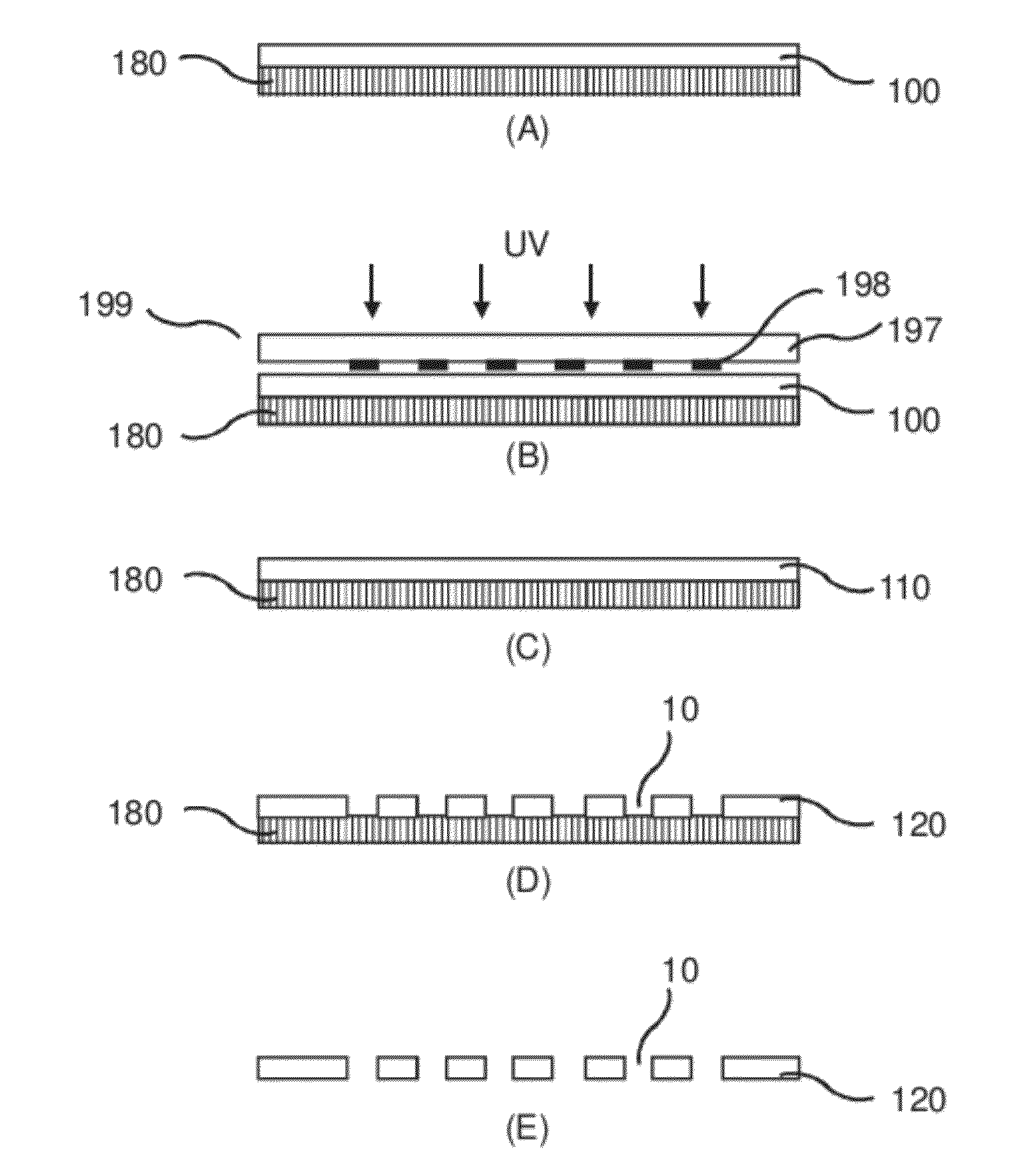
[0125]a. Laminate positive resist dry film on the copper[0126]b. Expose the positive resist dry film to UV though the microfilter optical mask. The parts of the positive resists that are exposed to the UV can be dissolved by developer.[0127]b. Develop the positive resist to form pores.[0128]c. Wet etch copper to release the microfilters.

[0129]2. Fabricate Microfilters from a Roll of Negative Resists Dry Film Using UV Lithography

example 2

Microfilter Fabrication Using a Roll of Negative Resist Dry Film

[0130]The negative resist dry film, such as PerMX™ 3000 series, is manufacture in roll form. To perform UV lithography of the resist in the role form as shown in FIG. 3 can simplify the fabrication. The method of implementation and steps of fabrication are described below.[0131]a. Between each exposure, an unexposed portion of a roll of negative resist dry films is advanced as shown in FIG. 5A. The films 102 laminated on removable substrate 182 are connected by rolls 175. They are stretched by rollers 170. The rolls advance by the distance appropriate for the optical mask and exposure system as indicated by arrow. During film advance, the optical mask 199 and support 191 are moved away from the films.[0132]b. During exposure, the stretched film 102 is pushed into the support 191 to provide additional tension and stability as shown in FIG. 5B. The UV exposure is performed after the optical mask 199 is placed on the films...

example 3

Fabrication Microfilters in a Roll of Negative Resist Dry Film and Applying Electrostatic Chuck to Fix the Films

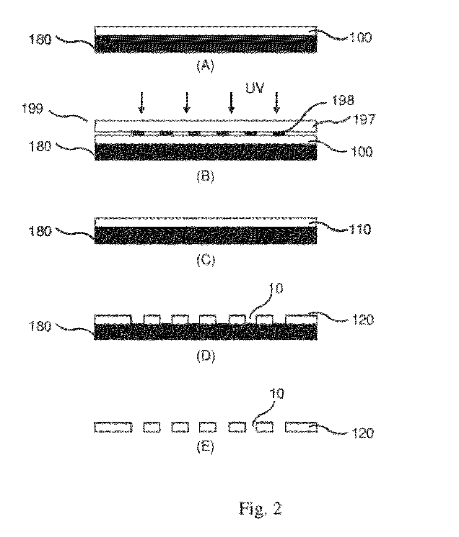
[0161]In FIG. 12, the concept of using electrostatic force to hold the films secure is shown, but the rollers are not shown. In FIG. 12A, the configuration of the system is shown between exposures. The one or more laminated negative resist film 200 laminated to post bake support film 280 to form films 201. A stack of films 201 are stretched. The substrate structure consist of a support 292, an insulator 267 and a conduction layer 266. A clear conducting film 265 is placed on top of the film. Voltage 269 is set to zero and the circuit is open.

[0162]FIG. 12B shows the configuration during exposure, where a voltage 169 is applied between the electrodes 265 and 266. This allows the films to be tightly fixed between the electrodes to avoid motion. The x-ray mask is place adjacent to the electrode 265 and exposure is performed.

[0163]If the films are not pre-laminated, finish fab...


PUM

PropertyMeasurementUnit
diameteraaaaaaaaaa
diameteraaaaaaaaaa
angleaaaaaaaaaa

Abstract

Micro- and nanofilters with precision pore sizes and pore layout have applications in many fields including capturing circulating tumor cells and fetal cells in blood, water treatment, pathogen detection in water, etc. Methods to fabricate micro- and nanofilters not using track etching or reactive ion etching are provided, allowing easy fabrication of single layer or stack of films simultaneously, and / or stack of films on rolls. Microfilter can be made using one or more layers of material. Invention enables mass production of microfilters with lithographic quality at low cost. Isolation, enumeration and characterization of circulating tumor cells using microfilters provides (i) guides to cancer treatment selection and personalize dosage, (ii) low cost monitoring for treatment response, disease progression and recurrence, (iii) assessment of pharmacodynamic effects, (iv) information on mechanisms of resistance to therapy, and (v) cancer staging. Microfabrication methods are also applicable to fabrication of any free standing patterned polymeric films.

Description

[0001]This application claims benefit under 35 U.S.C. §119 from U.S. Provisional Application No. 61 / 430,818, filed on Jan. 7, 2011, the entire content of which is incorporated herein by reference.[0002]The present invention relates to U.S. Provisional Patent Application Ser. No. 61 / 330,819, filed May 3, 2010 and U.S. Provisional Patent Application Ser. No. 61 / 377,797, filed Aug. 27, 2010 the entire contents of which are incorporated herein by reference.FIELD OF THE INVENTION[0003]The invention relates to method to fabricate high-aspect-ratio precision nanopores and nanopillars in photo sensitive polymer films over large area by optical interference lithography using ultra-violet radiation. Free standing nanopores in polymer films with aspect ratio over 30 have been demonstrated in films greater than 10 micron thick. Interference lithography provides the same periodic pattern over the large area and through the entire film thickness.[0004]The invention relates to method to fabricate ...

Claims


Application Information

Patent Timeline
Patent Type & Authority Applications(United States)
IPC IPC(8): C12Q1/04G03F7/20C12N5/078C12N5/077C12Q1/68G01N21/64C12Q1/25C12N5/071C12M1/12B01D61/14B01D61/18B01D61/24B32B3/26B01D39/00C12N5/09
CPCA61M1/16B01D67/0027B01D61/147B01D67/0034B01D69/12C12M47/02G01N21/6428G03F7/2022B01D67/0088B01D71/46B01D71/64B01D2323/34B01D2325/02B01D2325/08A61M1/34Y10T428/249978
Inventor TANG, CHA-MEIMAKAROVA, OLGA
Owner CREATV MICROTECH
Why Eureka
Try Eureka