Method of manufacturing silicon carbide semiconductor device

Active Publication Date: 2012-07-19
SUMITOMO ELECTRIC IND LTD
View PDF19 Cites 12 Cited by
  • Summary
  • Abstract
  • Description
  • Claims
  • Application Information

AI Technical Summary

Benefits of technology

[0008]According to the manufacturing method above, before annealing, the Al atoms contained in the contact electrode are present not as an element but as an alloy with at least any of Si atoms and Ti atoms. Thus, diffusion of the Al atoms to the outside of the contact electrode during annealing can be suppressed. Since diffusion of the Al atoms into the insulating film can thus be suppressed, insulation reliability of the insulating

Problems solved by technology

In a case where a contact electrode having Al atoms is arranged in contact with an insulating film, Al atoms in the contact electrode may

Method used


Image

  • Method of manufacturing silicon carbide semiconductor device
  • Method of manufacturing silicon carbide semiconductor device
  • Method of manufacturing silicon carbide semiconductor device

Examples


first embodiment

[0040]Initially, a construction of a MOSFET (Metal Oxide Semiconductor Field Effect Transistor) in the present embodiment will be described.

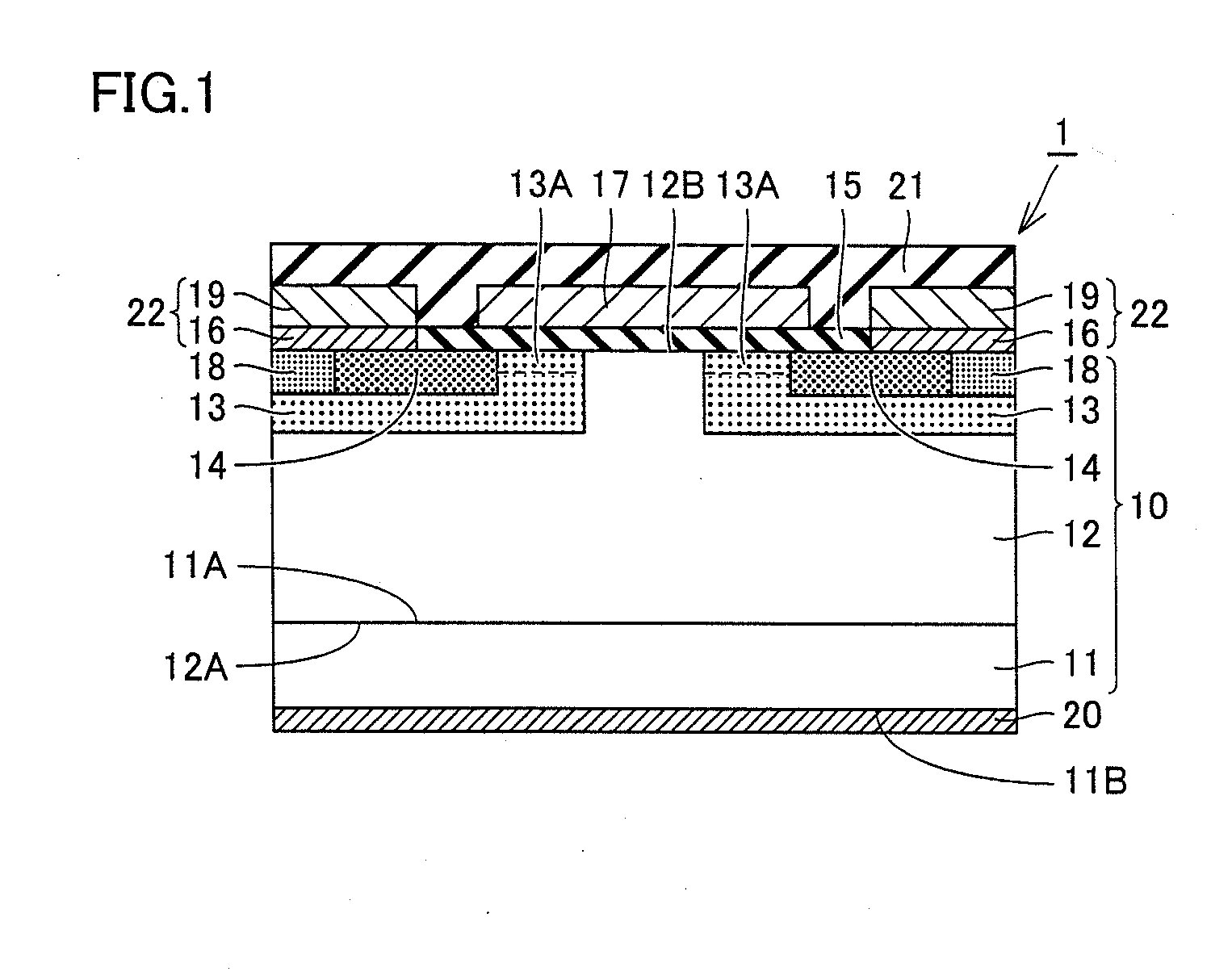
[0041]Referring to FIG. 1, a MOSFET 1 (a silicon carbide semiconductor device) has a silicon carbide substrate 10. Silicon carbide substrate 10 includes an n+ substrate 11, an n− SiC layer 12, a p body 13, an n+ source region 14, and a p+ region 18.

[0042]N+ substrate 11 is a substrate composed of silicon carbide (SiC) and having an n conductivity type. N+ substrate 11 contains an n-type impurity (an impurity having the n conductivity type) such as N (nitrogen) at high concentration.

[0043]N− SiC layer 12 is a semiconductor layer composed of SiC and having the n conductivity type. N− SiC layer 12 is formed on one main surface 11A of n+ substrate 11, for example, to a thickness of approximately 10 μm. Examples of n-type impurities contained in n− SiC layer 12 include N (nitrogen), and an impurity is contained at concentration lower than concentrati...

second embodiment

[0076]A construction of a JFET (junction field effect transistor) in the present embodiment will initially be described.

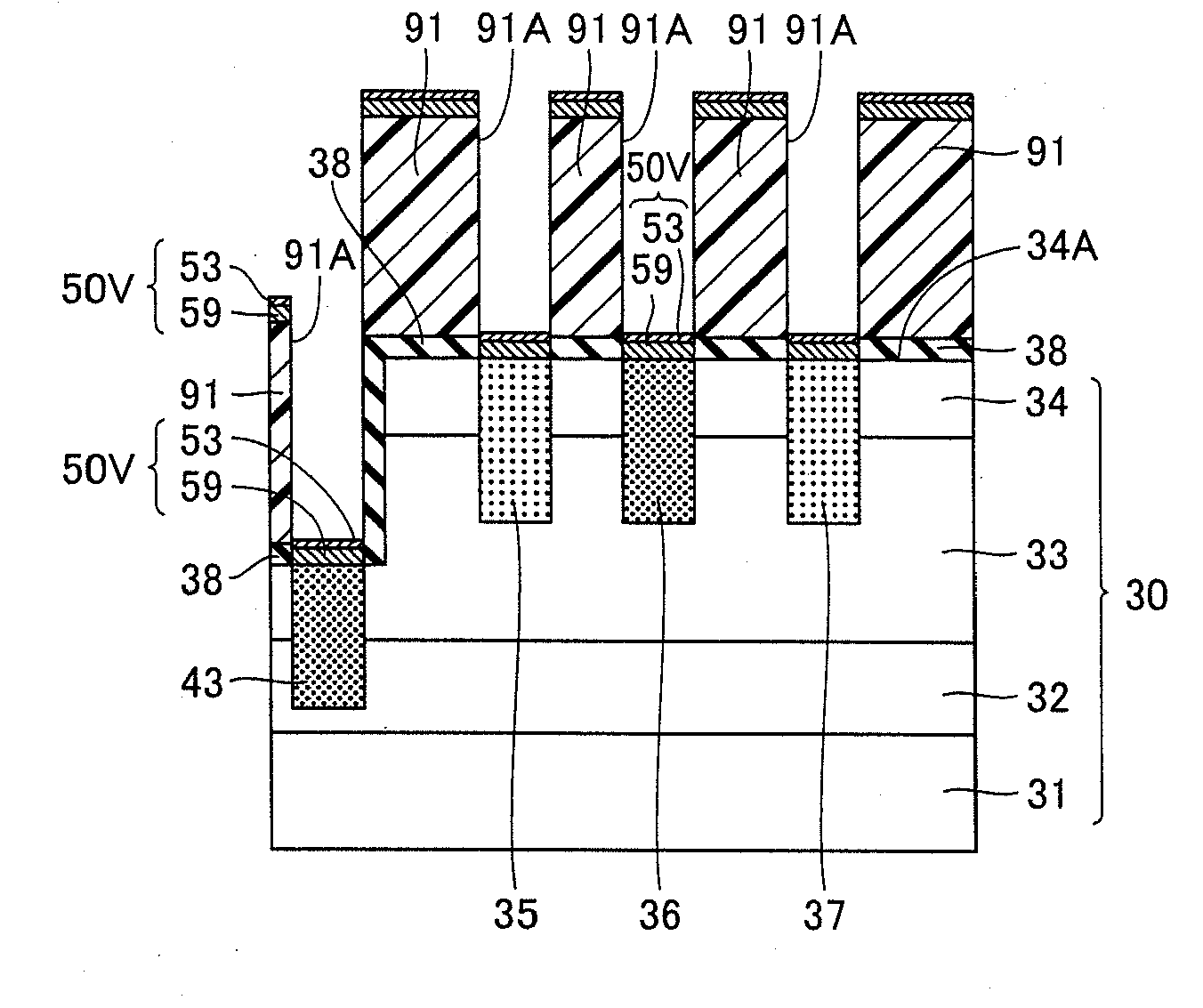
[0077]Referring to FIG. 10, a JFET 3 (a silicon carbide semiconductor device) is similar in construction of an ohmic contact electrode to MOSFET 1 in the first embodiment above, and achieves similar effects. Specifically, JFET 3 has a silicon carbide substrate 30. Silicon carbide substrate 30 has an n-type substrate 31, a first p-type layer 32, an n-type layer 33, and a second p-type layer 34. N-type substrate 31 is composed of SiC and has the n conductivity type. First p-type layer 32 is formed on n-type substrate 31. N-type layer 33 is formed on first p-type layer 32. P-type layer 34 is formed on n-type layer 33. First p-type layer 32 can have a thickness of approximately 10 μm and concentration of a p-type impurity of approximately 7.5×1015 cm−3. For example, n-type layer 33 can have a thickness of approximately 0.45 μm and concentration of an n-type impurity of...

third embodiment

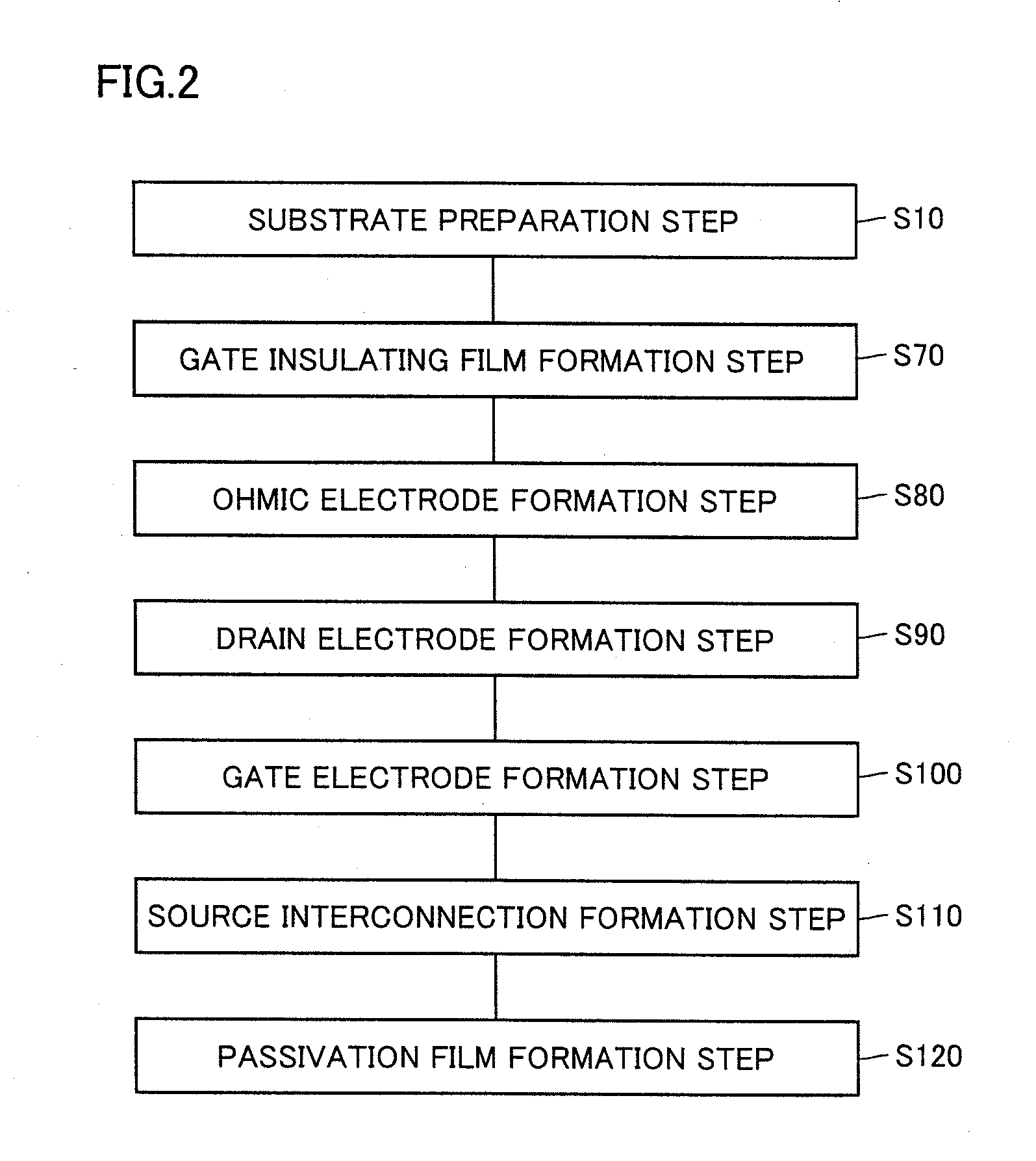
[0107]In the present embodiment as well, MOSFET 1 substantially the same as in the first embodiment is manufactured. Initially, as in the first embodiment, in gate insulating film formation step S70 (FIG. 2), gate oxide film 15 (insulating film) is formed.

[0108]Referring to FIG. 19, in an Al—Si alloy film formation step S82 (FIG. 18), an alloy film 59 made of an alloy containing Al atoms and Si atoms is formed. Namely, alloy film 59 is formed on second main surface 12B and on the main surface of n+ substrate 11 opposite to n− SiC layer 12. Preferably, the alloy film is formed with sputtering using a sputtering target 99. Sputtering target 99 is made of an alloy containing Al atoms and Si atoms.

[0109]Referring to FIG. 20, then, in a Ti film formation step S83 (FIG. 18), a Ti film 53 is formed on alloy film 59. Thus, a stack film 50V having alloy film 59 and Ti film 53 is formed.

[0110]Referring further to FIG. 21, then, as a result of removal of resist film 91, stack film 50V on resis...


PUM


Abstract

A silicon carbide substrate having a substrate surface is prepared. An insulating film is formed to cover a part of the substrate surface. A contact electrode is formed on the substrate surface, so as to be in contact with the insulating film. The contact electrode contains Al, Ti, and Si atoms. The contact electrode includes an alloy film made of an alloy containing Al atoms and at least any of Si atoms and Ti atoms. The contact electrode is annealed such that the silicon carbide substrate and the contact electrode establish ohmic connection with each other. Thus, in a case where a contact electrode having Al atoms is employed, insulation reliability of the insulating film can be improved.

Description

BACKGROUND OF THE INVENTION[0001]1. Field of the Invention[0002]The present invention relates to a method of manufacturing a silicon carbide semiconductor device, and more particularly to a method of manufacturing a silicon carbide semiconductor device having a contact electrode containing Al atoms.[0003]2. Description of the Background Art[0004]WO2009 / 128419 (Patent Literature 1) discloses a material containing titanium (Ti) and aluminum (Al) as a material for an ohmic contact electrode arranged in contact with an SiC wafer (a silicon carbide substrate). According to this publication, a contact resistance with the SiC wafer can be lowered by applying the material above.[0005]In a case where a contact electrode having Al atoms is arranged in contact with an insulating film, Al atoms in the contact electrode may diffuse into the insulating film during annealing treatment, which may result in lowering in insulation reliability of the insulating film. Then, an object of the present inv...

Claims


Application Information

Patent Timeline
IPC IPC(8): H01L21/28
CPCH01L29/1608H01L29/45H01L29/66068H01L21/0485H01L29/7802H01L29/808H01L21/046H01L29/66901H01L21/28H01L21/18
Inventor YAMADA, SHUNSUKE
Owner SUMITOMO ELECTRIC IND LTD
Why Eureka
Try Eureka