

Coated polymer dielectric film
a technology of dielectric film and coating, applied in the direction of plastic/resin/waxes insulators, natural mineral layered products, instruments, etc., can solve the problems of limiting the operating voltage of electronic devices, thermal stability, and reducing lifetim
- Summary
- Abstract
- Description
- Claims
- Application Information
AI Technical Summary
Benefits of technology
Problems solved by technology
Method used
Image

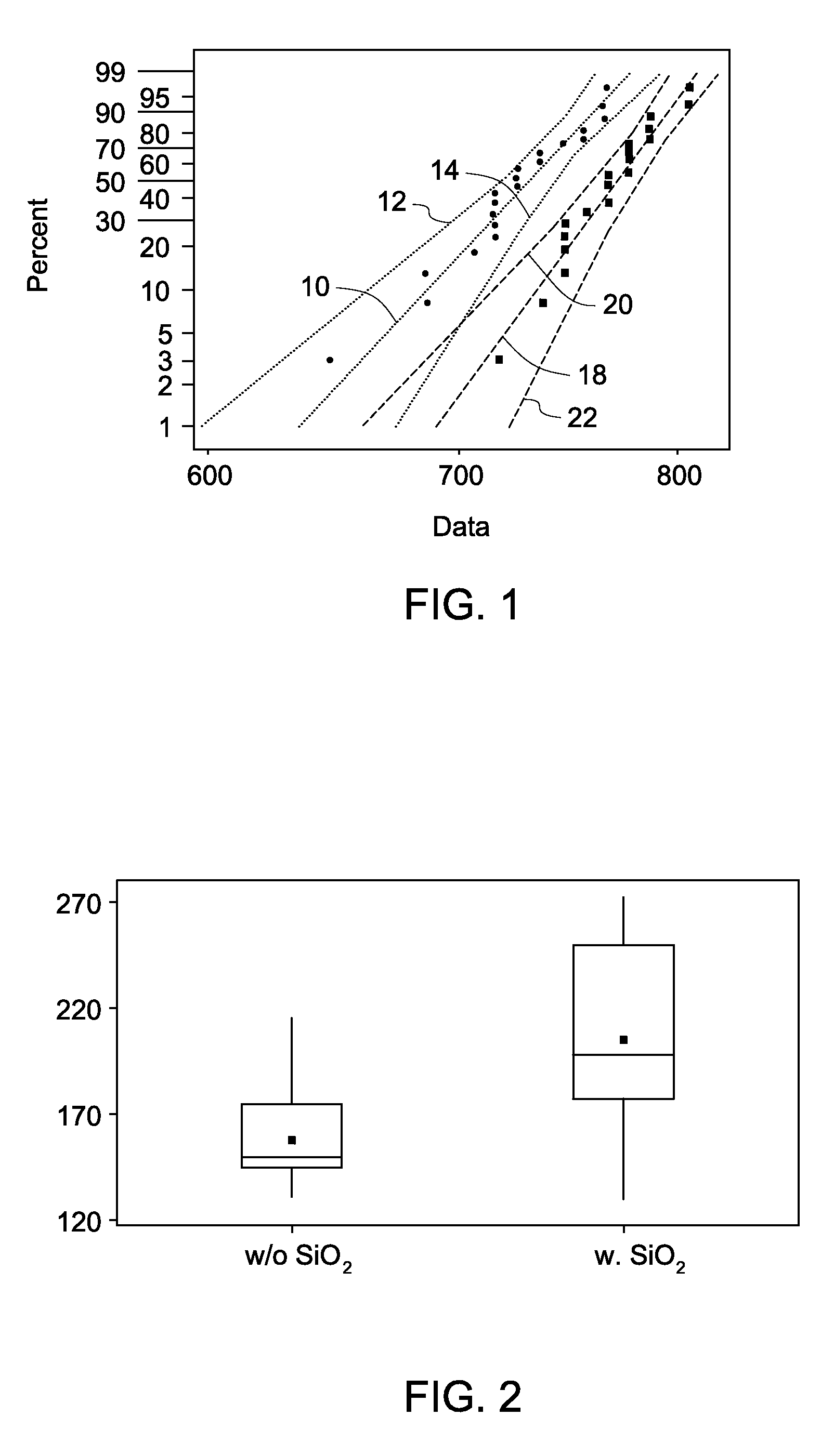
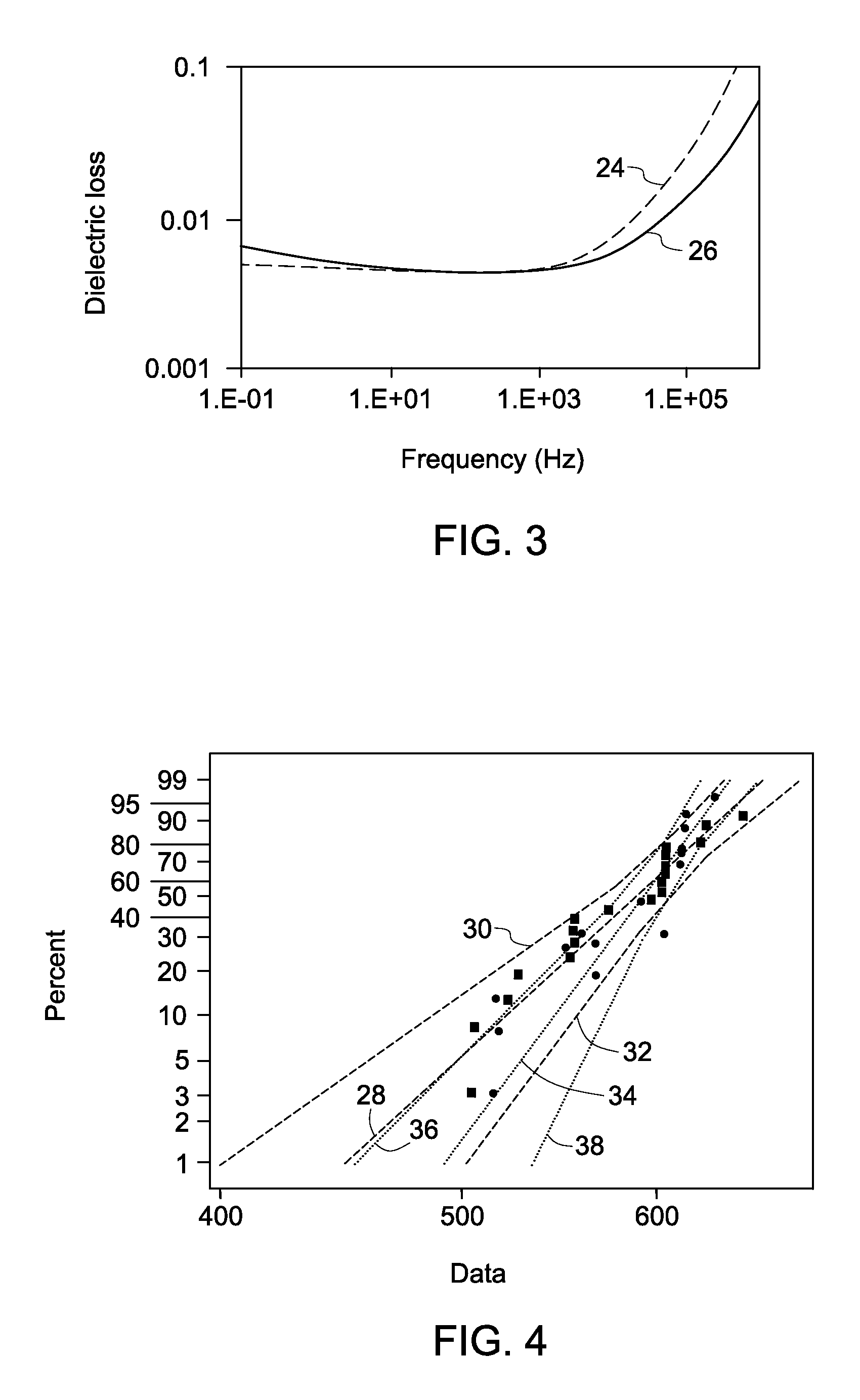
Examples
examples
[0042]The following examples illustrate methods and embodiments in accordance with the invention, and as such, should not be construed as imposing limitations upon the claims.
[0043]Unless specified otherwise, all ingredients may be commercially available from such common chemical suppliers as Alpha Aesar, Inc. (Ward Hill, Mass.), Sigma Aldrich (St. Louis, Mo.), Spectrum Chemical Mfg. Corp. (Gardena, Calif.), and the like.
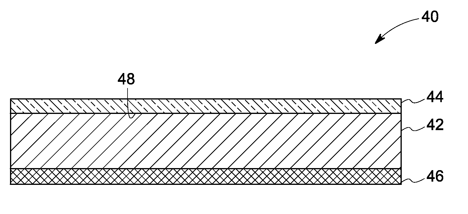
[0044]The polyetherimide polymer films are commercially available from Mitsubish Plastics, Inc. The films are used as substrate for the coating materials such as SiO2 and SiNx. The film thicknesses used in the following examples are 13 um and 25 um.
Sputter Deposition of SiO2 layer
[0045]A Perkin Elmer Model 4450 sputtering machine was used to deposit SiO2 coating on the first polymer layer. The sputtering targets of SiO2 were fixed inside the sputtering system and cleaned thoroughly. The polymer first layer was hooped on a metal ring to keep the film from winkling an...
PUM
| Property | Measurement | Unit |
|---|---|---|
| thickness | aaaaa | aaaaa |
| thickness | aaaaa | aaaaa |
| thickness | aaaaa | aaaaa |
Abstract
Description
Claims
Application Information