Surface emission laser

a laser and surface technology, applied in the field of surface emission lasers, can solve the problems of difficult to obtain high optical output, short cavity length, and inconvenient multi-channel high-density mounting and downsizing of the entire module, and achieve the effect of reducing the increase of parasitic capacity, improving radiation performance, and reducing the parasitic capacity

Inactive Publication Date: 2012-09-13
HITACHI LTD
View PDF2 Cites 13 Cited by
  • Summary
  • Abstract
  • Description
  • Claims
  • Application Information

AI Technical Summary

Benefits of technology

[0024]According to an aspect of the present invention, the first electrode is directly formed on the first conductive layer laminated on the substrate, and no pn junction is provided immediately below. Therefore, it is possible to significantly suppress an increase in the parasitic capacity when the area of an electrode is expanded. Thus, by employing a mounting structure in which the supporting member such as a metal member is brought into contact with the first electrode part to form a radiation path, the radiation performance can be considerably improved without increasing the parasitic capacity. Further, a contact area between the electrode and the semiconductor can be increased, so that the contact resistance can be advantageously reduced and the resistance of the element can be also reduced.
[0025]Further, the element can be mounted in a flip-chip manner on the optical element mounting substrate having electric lines provided, and thus attenuation of a high-frequency signal caused by inductance can be reduced as compared to a case of using gold wires.
[0026]Furthermore, it is possible to design impedance matching with the use of patterning of the electric lines, and the degree of freedom of electric design can be considerably enhanced. Thus, the present invention is advantageous in high speed.

Problems solved by technology

With such a background, improvement of high-speed performance and simple and high-density mounting are important issues for a semiconductor optical element transmitting and receiving signals.
However, it is necessary to install an optical member for receiving laser light in the surface of the mounting substrate while being adjacent to the laser element, and thus the laser is not suitable for multi-channel high-density mounting and downsizing of the entire module.
In the case of this structure, however, the length of the cavity is extremely short because it is determined on the basis of the thickness of a crystal growth film, and it is essentially difficult to obtain high optical output.

Method used


Image

  • Surface emission laser
  • Surface emission laser
  • Surface emission laser

Examples


first embodiment

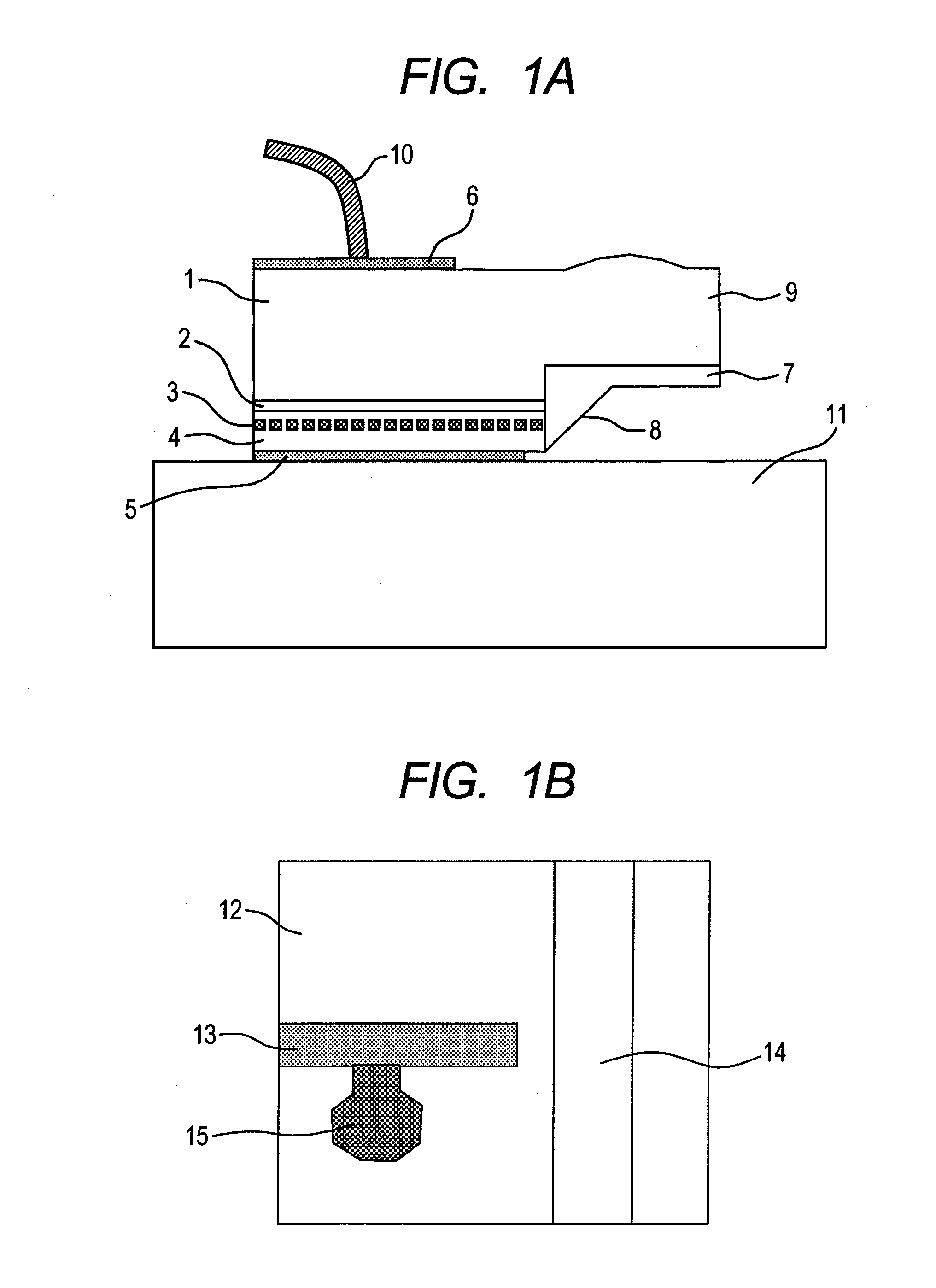
[0051]A structure of a horizontal-cavity surface-emitting laser according to a first embodiment will be described using FIG. 2A, FIG. 2B, FIGS. 3A to 3F, and FIGS. 4A to 4C. The embodiment is an example of applying the present invention to a horizontal-cavity surface-emitting laser with a width of 250 μm. FIG. 2A is a birds-eye view of a surface of a laser element, and FIG. 2B shows a light emitting surface of the laser element. The horizontal-cavity surface-emitting laser of the embodiment is formed in such a manner that an n-type semiconductor layer 21, an active layer 22, and a p-type semiconductor layer 23 are laminated and grown in this order on an Fe-doped semi-insulating semiconductor substrate 20, and further a diffraction grating layer (not shown) is formed directly on the active layer 22. N-doped InP is used for the n-type semiconductor layer 21, p-doped InP is used for the p-type semiconductor layer 23, and, for example, a strain quantum well structure of InGaAlAs is used...

second embodiment

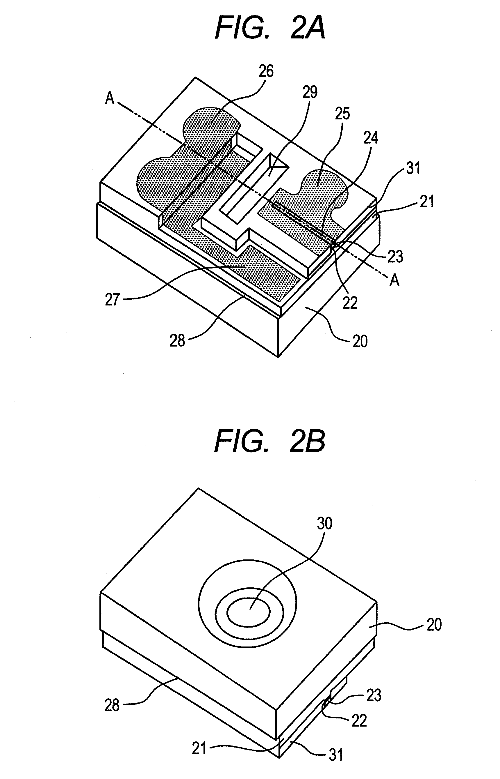
[0077]A second embodiment is an example in which the present invention is applied to an RWG-type horizontal-cavity surface-emitting laser with a width of 250 μm. FIG. 5A is a birds-eye view of a surface of the laser element, and FIG. 5B shows a light emitting surface. Further, FIG. 5C is a cross-sectional view in the direction orthogonal to the optical axis in which the laser element is mounted. The structure of the laser element will be described in detail using FIG. 5A and FIG. 5B. The laser element is formed in such a manner that an n-type semiconductor layer 4001, an active layer 4002, and a p-type semiconductor layer 4003 are laminated and grown in this order on an Fe-doped semi-insulating semiconductor substrate 4000, and further a diffraction grating layer (not shown) is formed directly on the active layer 4002. N-doped InP is used for the n-type semiconductor layer 4001, p-doped InP is used for the p-type semiconductor layer 4003, and, for example, a strain quantum well stru...

third embodiment

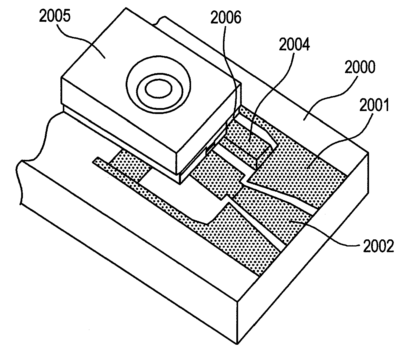
[0083]FIG. 6 shows a third embodiment in which the present invention is applied to the horizontal-cavity surface-emitting laser. FIG. 6 is a birds-eye view of the laser element. The embodiment is an array-type laser in which plural horizontal-cavity surface-emitting lasers were formed on the same substrate. In the embodiment, a 4-channel parallel structure was employed. Further, the RWG type or the BH type may be employed. However, the embodiment employed the RWG type. Laser elements 3003 forming the 4-channel array are electrically separated from each other through the electricity separation groove 4008 as shown in the single laser element of FIG. 3. The manufacturing method is the same as the second embodiment. It should be noted that the substrate used in the embodiment was a semi-insulating semiconductor substrate, but a lamination structured substrate formed using semi-insulating semiconductor layers and conductive semiconductor layers may be used. In such a lamination structur...


PUM


Abstract

Specifically, provided is a horizontal-cavity surface-emitting laser including, on a semiconductor substrate: a cavity structure; a waveguide layer; and a reflecting part, wherein a first electrode provided on the semiconductor substrate along side regions of the cavity structure and the reflecting part and a second electrode provided on the main surface of the cavity structure are provided, the first electrode includes an electrode (1) that is provided around one side region of the reflecting part located in the direction intersecting with the traveling direction of light guided through the waveguide layer and an electrode (2) provided around one side region of the cavity structure and the other side region of the reflecting part that are located in the direction parallel with the traveling direction of light guided through the waveguide layer, and the shape of the electrode (2) has different widths at at least two positions.

Description

TECHNICAL FIELD [0001]The present invention relates to a semiconductor laser element used for optical communications, an optical disk, a medical sensor, and the like, and an optical module using the same.BACKGROUND ART[0002]With the development of information technology, communication traffic through which large-volume data is transmitted and received at high speed using light is beginning to be rapidly prepared. In particular, the volume of data has been significantly increased not only in conventional communication networks (telecommunications), but also in data communications such as Storage Area Network (SAN) and Ethernet (registered trademark) (LAN), and high-speed communications using light have been actively progressed. For example, the communication standard of 100-gigabit Ethernet for transmitting 100-gigabit data is beginning to be designed in the next-generation optical LAN.[0003]Further, the throughput of a recent high-end router used in a backbone system reaches as high...

Claims


Application Information

Patent Timeline
Patent Type & Authority Applications(United States)
IPC IPC(8): H01S5/18H01S5/185H01S5/02375H01S5/12
CPCH01S5/02212H01S5/0224H01S5/02268H01S5/02284H01S5/0267H01S5/4025H01S5/12H01S5/18H01S5/2224H01S5/4031H01S5/0425H01L2224/73265H01L2924/10155H01S5/04257H01S5/04256H01S5/02375H01S5/0234H01S5/02345H01S5/02251H01S5/185
Inventor ADACHI, KOICHIROMATSUOKA, YASUNOBUSUGAWARA, TOSHIKISHINODA, KAZUNORITSUJI, SHINJI
Owner HITACHI LTD
Why Eureka
Try Eureka