Method and apparatus for depositing a thin film

a thin film and deposition method technology, applied in the field of thin film deposition, can solve the problems of poor energy conversion efficiency that does not yield a cost benefit, limited fossil fuel supply, and insufficient to meet the ever-growing demand for this source of energy, and achieves the effects of reducing the reaction rate and throughput, extending the capability of existing equipment, and reducing the effect of gas phase and surrounding surfa

Inactive Publication Date: 2012-09-20
2 PYE SOLAR
View PDF6 Cites 38 Cited by
  • Summary
  • Abstract
  • Description
  • Claims
  • Application Information

AI Technical Summary

Benefits of technology

[0009]In several preferred thin film deposition methods of the present invention, only the substrate is heated, which in turn provides the energy for thermal pyrolysis of the reactant gases to form the deposited film as they contact the substrate. The substrate is heated to a temperature desirable for large scale commercial production deposition rates and film properties. By heating only the substrate, reaction in the gas phase and on surrounding surfaces is minimized. This has the beneficial effect of significantly extending the capability of existing equipment for higher deposition rates and throughput while minimizing down time for cleaning.
[0010]Further, the focused pyrolytic deposition method of the present invention will allow uniform large area deposition of silicon absorber films at high temperature and high deposition rate yielding high throughput of near crystalline quality in a cold-wall system where the reaction is limited to the hot substrate rather than depositing everywhere and depleting non-uniformly with uncontrolled gas phase reaction. Other films suitable as additional layers in a photovoltaic solar cell, such as barrier, passivation or anti-reflective coatings may also be deposited using additional embodiments of the present invention. These films may be deposited, for example, in sequence in one open, in-line system. The methods of the present invention are not only applicable in photovoltaics, but also for semiconductors, opto-electronic, integrated circuit and other applications.

Problems solved by technology

The supply of fossil fuels, such as oil and coal, is limited and will not be sufficient to meet the ever rising demand for this source of energy.
Photovoltaic solar cells made from crystalline materials often have better rates of converting electromagnetic radiation into electrical power and better reliability than those made with conventional thin film technology, but are often costly and difficult to manufacture on a large scale.
For example, crystalline silicon is well established and characterized as a reliable photovoltaic absorber material, but many techniques attempting to manufacture a thin film version of a silicon solar cell to reduce material costs suffer from poorer energy conversion efficiency that does not yield a cost benefit.
Additionally, desirable material properties are often only achieved by utilizing a sufficiently high temperature for a complete chemical reaction either during deposition or in a subsequent annealing process.
However, current thermal deposition technology suffers from uncontrolled reaction on all exposed surfaces or parasitic reaction in the gas phase yielding poor film quality with rapid depletion degrading uniformity when attempting to cover large substrate areas as the deposition rate is increased with temperature or chemical concentration.
Using plasma or photolytic interaction to activate the reaction in the gas phase at a lower substrate temperature suffers the same problems when attempting to increase the deposition rate significantly.
Limitations to existing thin film deposition technology have so far made it economically impractical to generate production volume quantities of a silicon absorber film having near crystalline quality in a thin film form to yield unsubsidized competitive photovoltaic solar cells.

Method used


Image

  • Method and apparatus for depositing a thin film
  • Method and apparatus for depositing a thin film
  • Method and apparatus for depositing a thin film

Examples


Embodiment Construction

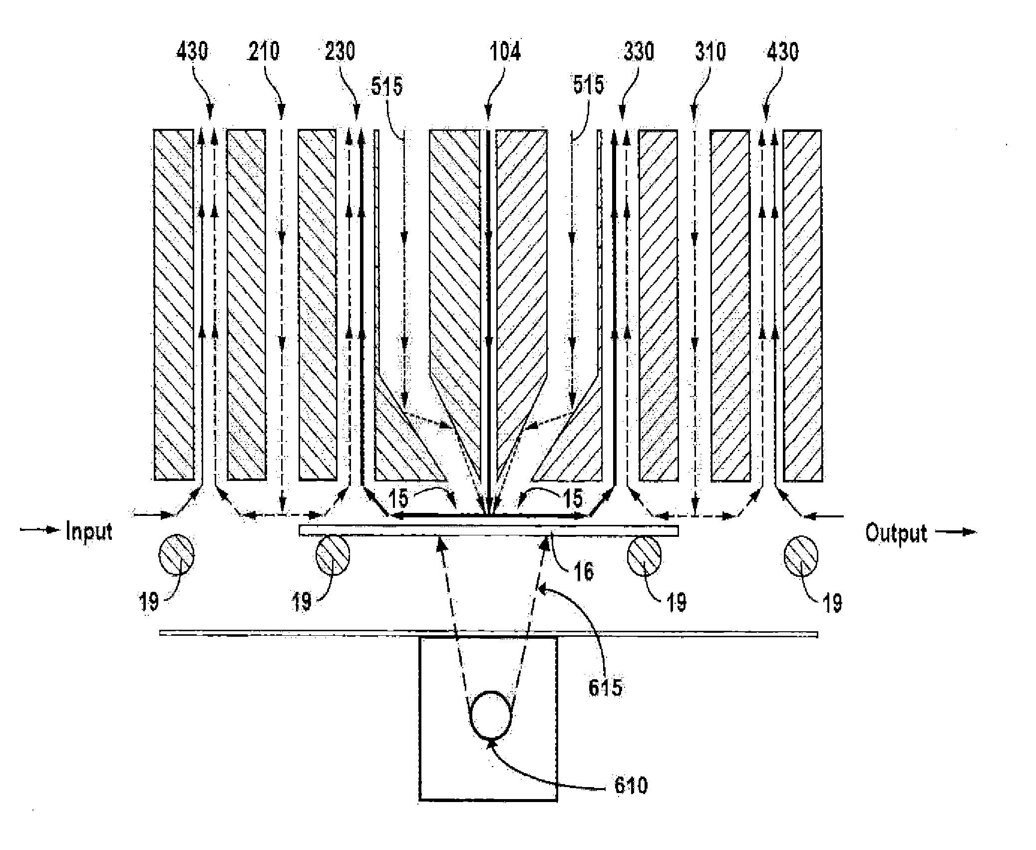
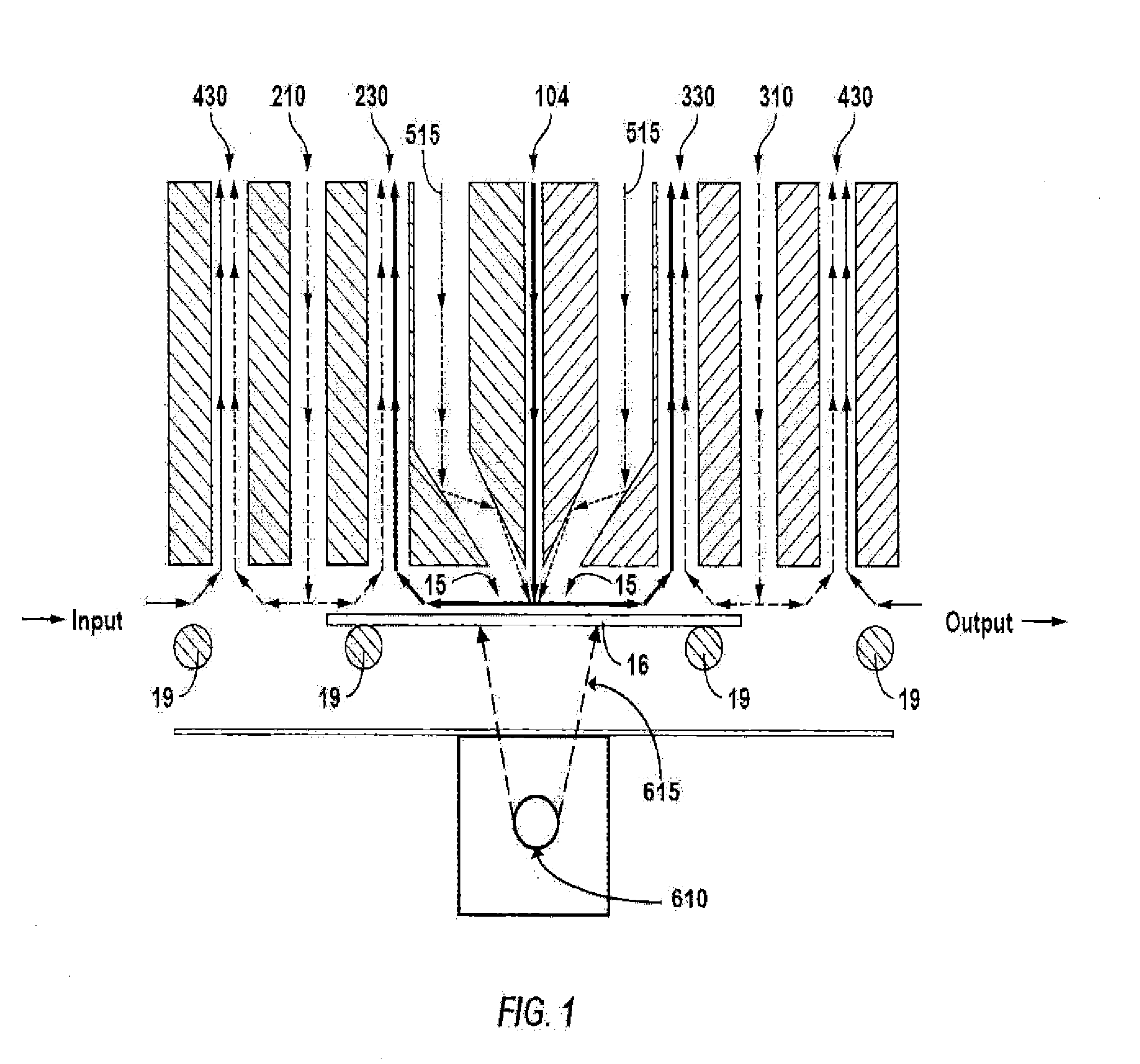
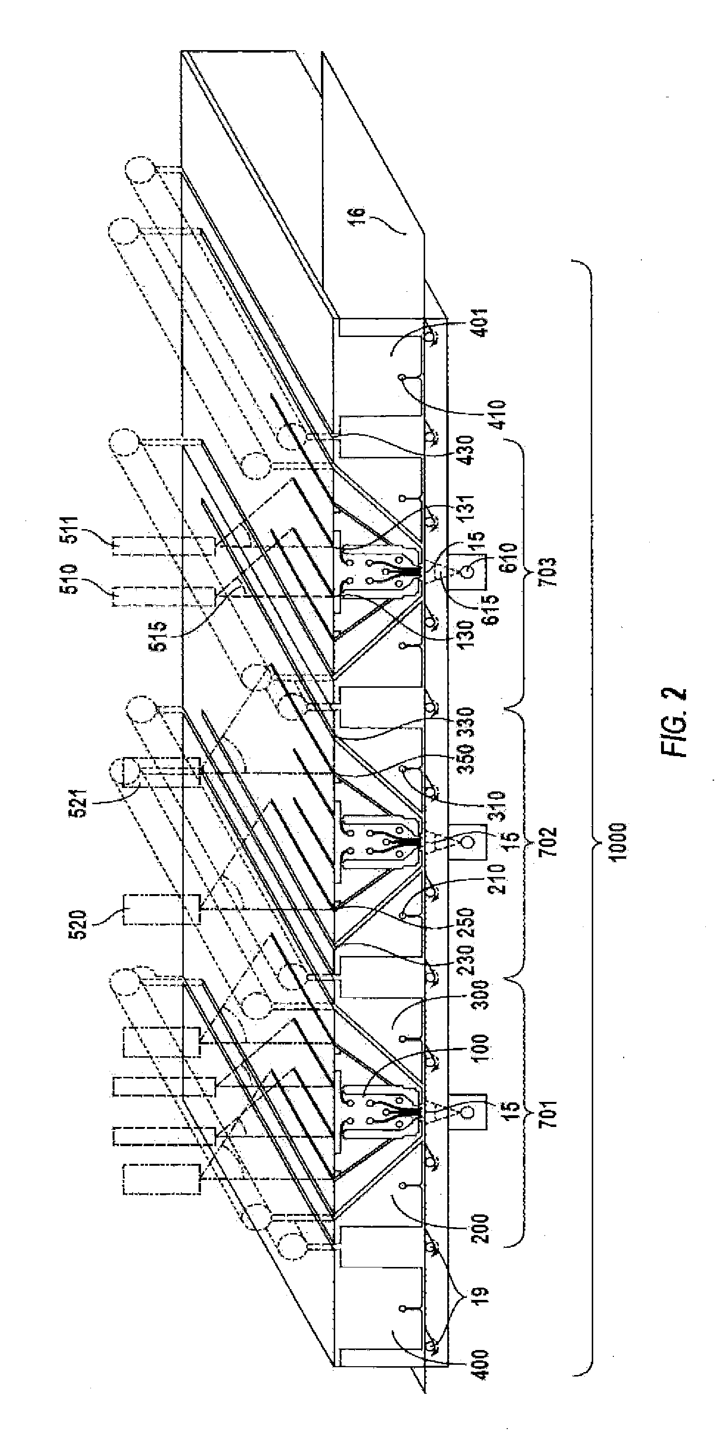
[0022]In accordance with one embodiment of the present invention, a thin film or a multitude of film layers are deposited on a substrate by injecting chemical gases directly and locally on the surface of the substrate while the substrate surface is locally heated by a light beam applied to the opposite surface of the substrate. In other words, if the chemical gases are deposited on top of the substrate, heat is applied by a light beam situated under the substrate (or vice-versa). In this embodiment, the objective is to have the chemical deposition occur by thermal pyrolysis rather than photolytic interaction.

[0023]In some embodiments, the substrate is moved at a constant speed relative to a line source injecting the chemical gas. Film deposition may be carried out at or near atmospheric pressure in a chamber that is purged using an inert gas. Continuous processing in an open in-line system may be carried out in a controlled atmosphere using inert gas purge for isolation from ambient...


PUM

PropertyMeasurementUnit
temperatureaaaaaaaaaa
surface areaaaaaaaaaaa
wavelengthsaaaaaaaaaa

Abstract

A substrate is brought into close proximity with one or more gas injectors to deposit a thin film. As the substrate is moved horizontally along a predefined direction, it is injected with reactive gases and pyrolytically heated with a heating light focused on the substrate. To prevent photolytic reactions, the heating light source is preferably on the side of the substrate opposite to the side where the reactive gases are deposited. In some embodiments, this heating light source is supplemented by heating light sources on the same side of the substrate as the deposited reactive gases. The heating light source(s) has a wavelength to optimize absorption by the substrate or the deposited film layer.

Description

CROSS-REFERENCED TO RELATED APPLICATIONS[0001]This application is a continuation-in-part of U.S. application Ser. No. 12 / 646,232, filed on Dec. 23, 2009, the disclosures of which are incorporated herein by reference in their entirety for all purposes.FIELD OF THE INVENTION[0002]The present invention relates to the field of thin film deposition and, more particularly, to atmospheric pressure deposition of thin films in an open in-line system during the manufacture of photovoltaic, semiconductor, opto-electronic, integrated circuit devices, and the like.BACKGROUND OF THE INVENTION[0003]The continuing rise in demand for energy, coupled with concerns about consequences of the increasing level of carbon dioxide in the atmosphere, has resulted in a drive to explore and harness alternative and renewable sources of energy. The supply of fossil fuels, such as oil and coal, is limited and will not be sufficient to meet the ever rising demand for this source of energy. Alternative sources of e...

Claims


Application Information

Patent Timeline
Patent Type & Authority Applications(United States)
IPC IPC(8): C23C16/46C08J7/18
CPCC08J7/08Y02E10/547C23C16/24C23C16/45578C23C16/45595C23C16/46C23C16/482C23C16/545H01L31/18H01L31/1804H01L31/1824H01L31/1868H01L31/1884Y02E10/545C08J7/123Y02P70/50
Inventor PYE, THOMASBARTHOLOMEW, LARRY
Owner 2 PYE SOLAR
Why Eureka
Try Eureka