Diamond Particle Mololayer Heat Spreaders and Associated Methods
- Summary
- Abstract
- Description
- Claims
- Application Information
AI Technical Summary
Benefits of technology
Problems solved by technology
Method used
Image

Examples
example 1
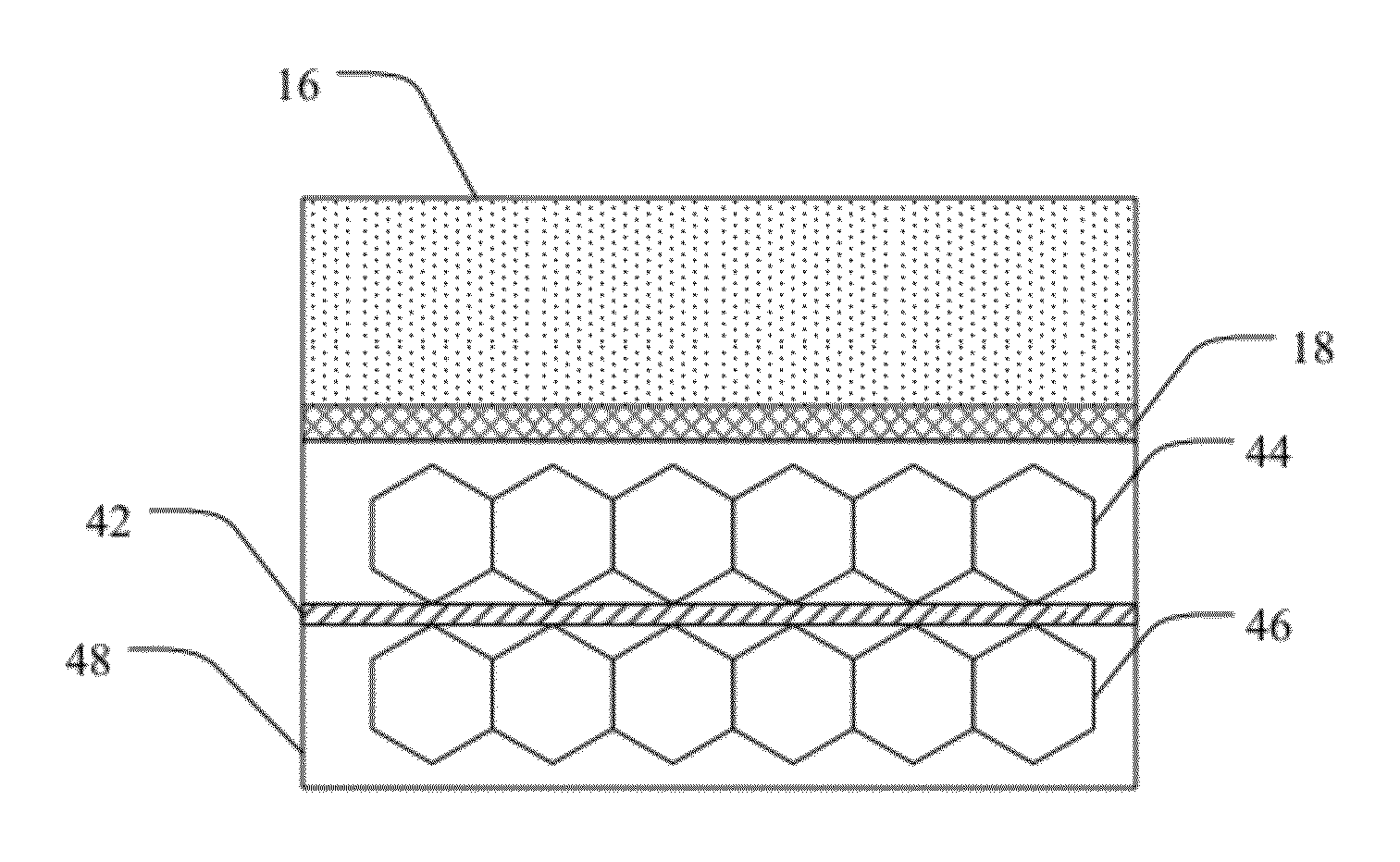
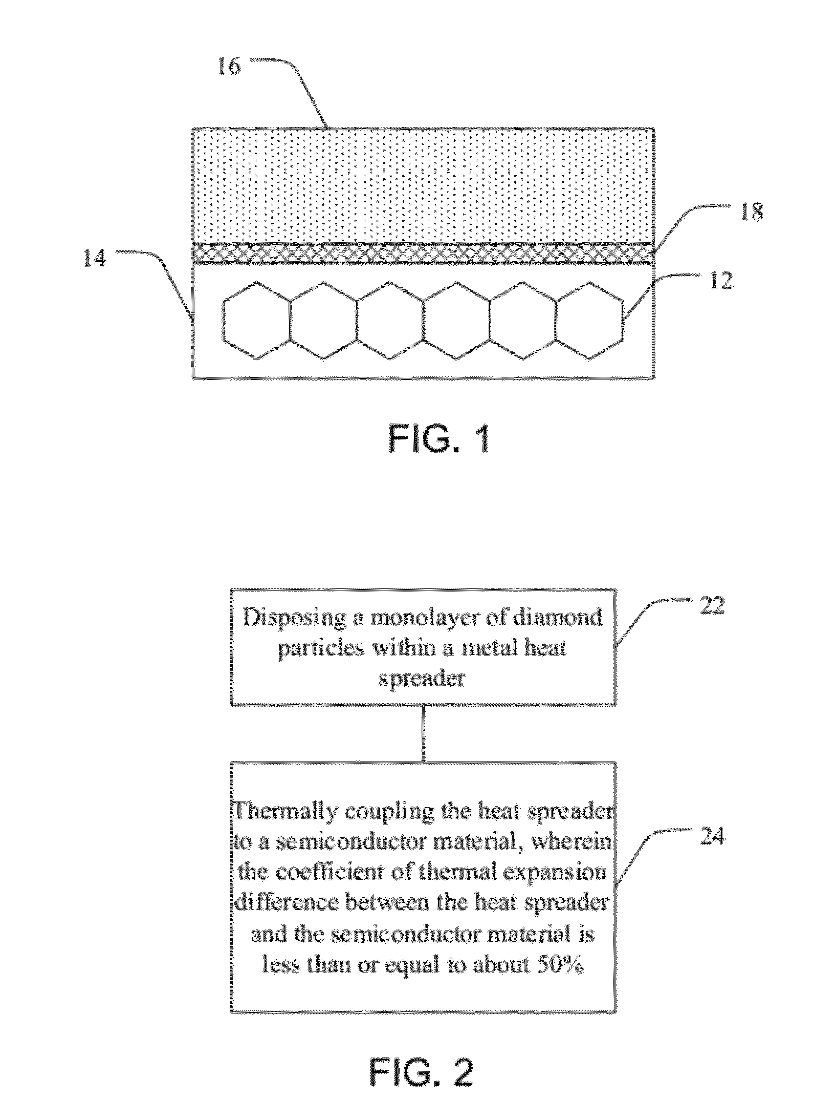
[0065]Ti coated diamond particles are arranged as a monolayer on a first copper metal layer. A second copper metal layer is placed on top of the diamond monolayer opposite to the first copper metal layer. This copper sandwich is hot pressed to make a copper heat spreader having a diamond particle monolayer at the center. Hydrogenated DLC is coated on one surface of the heat spreader as an insulating layer. It is sputter coated with Cr and Cu. The copper can be thickened by electroplating (e.g. to 35 microns). The copper layer can be etched to form circuits by lithography. An LED wafer with sapphire on one side and two electrodes on the other side is coupled to the etched circuits such that the two electrodes are separately bonded to two circuits.
example 2
[0066]An LED wafer with GaN on sapphire is metalized with gold. The copper heat spreader of Example 1 is soldered onto the metalized GaN. The sapphire is split off by laser irradiation, and the GaN material is coated with indium tin oxide (ITO) as a transparent electrode, with a small area where gold is coated as the anode. The copper heat spreader acts as the cathode. Such a vertical stack LED has opposing electrodes on opposing sides of the device, and can thus allow more efficient light emission due to reduced foot print and improved cooling.
example 3
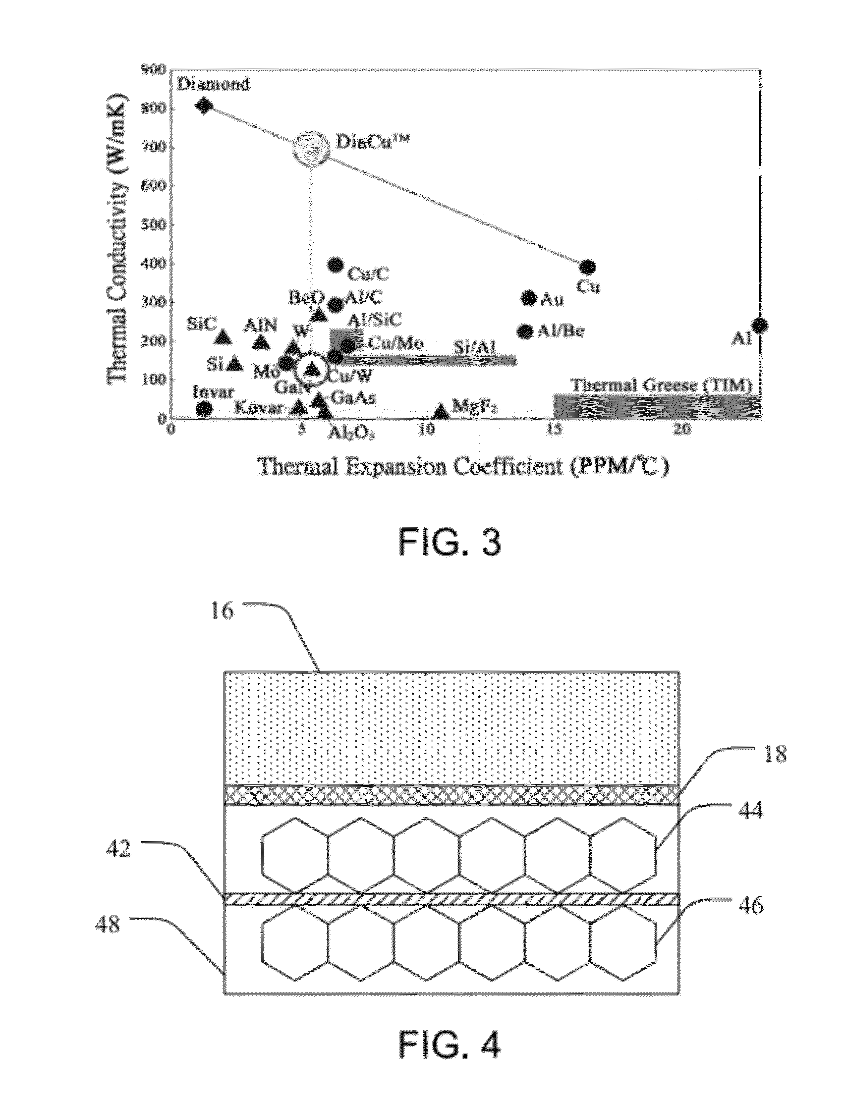
[0067]A thin metal layer (e.g. Cu 100 microns thick) has an adhesive (e.g. 3M manufacture, 25 microns, fugitive, i.e. can vaporize to leave no residue carbon behind) on each side. Ti coated diamond particles (e.g. about 50 microns) are spread on both sides create a diamond particle monolayer on each side. Excess diamond particles are removed. The layer is placed in a graphite mold that is covered with a thin layer of Cu powder. An additional layer of Cu powder is applied on top of the layer. The assembly is then hot pressed (e.g. 900 C for 20 minutes) under vacuum or in an inert atmosphere to form a flat disk with copper layers on both sides. Due to the presence of Ti coating, Cu can bond the diamond particles firmly. The flatness of the disk is maintained by the flat mold surface. The disk is then polished on both sides to make surfaces smooth. The resulting disk contains two layers of diamond in a copper matrix with high thermal conductivity and low CTE.
PUM
 Abstract
Description
Claims
Application Information
 - Generate Ideas
- Intellectual Property
- Life Sciences
- Materials
- Tech Scout
- Unparalleled Data Quality
- Higher Quality Content
- 60% Fewer Hallucinations
Browse by: Latest US Patents, China's latest patents, Technical Efficacy Thesaurus, Application Domain, Technology Topic, Popular Technical Reports.
© 2025 PatSnap. All rights reserved.Legal|Privacy policy|Modern Slavery Act Transparency Statement|Sitemap|About US| Contact US: help@patsnap.com