Chemical vapor deposition coating, article, and method

a technology of chemical vapor deposition and coating, applied in the chemical field, can solve the problems of inability to meet certain performance requirements, surface degradation in certain environments, and combinations, and achieve the effects of improving use, improving wear resistance and hardness, and reducing or eliminating residual catalyst activity

Active Publication Date: 2012-10-04
SILCOTEK CORP
View PDF5 Cites 45 Cited by
  • Summary
  • Abstract
  • Description
  • Claims
  • Application Information

AI Technical Summary

Benefits of technology

[0014]Another advantage of an embodiment is that the silicon, carbon, and hydrogen material is not susceptible to dissolution in high pH media.
[0015]Another advantage of an embodiment is that the oxidized materials display an improved wear resistant and hardness for improved use in environments with impact or sliding wear.
[0016]Another advantage of an embodiment is that use of an additional metal catalyst can be avoided in the formation of a coating including silicon, carbon, and hydrogen.
[0017]Another advantage of an embodiment is that residual catalyst activity is reduced or eliminated.
[0018]Another advantage of an embodiment is that steps for removal of catalyst can be eliminated.
[0019]Another advantage of an embodiment is the use of a non-pyrophoric substance that can improve safety.

Problems solved by technology

Often, surfaces of substrates do not include desired performance characteristics.
The failure to include specific desired performance characteristics can result in surface degradation in certain environments, an inability to meet certain performance requirements, or combinations thereof.
For example, in certain environments, metallic, glass, and ceramic surfaces can be subjected to undesirable surface activities such as chemical adsorption, catalytic activity, corrosive attack, oxidation, byproduct accumulation or stiction, and / or other undesirable surface activities.
Amorphous silicon-based chemical vapor deposition materials, however, are susceptible to dissolution by caustic high pH media, thereby limiting their use.
These materials are not wear resistant or hard enough for effective use in environments with impact or sliding wear.
Additionally, the functionalization of silicon materials with unsaturated hydrocarbons often requires the use of a metal catalyst.
Such processes suffer from the drawbacks that complete removal of this catalyst from the treated system is often difficult and the presence of the catalyst can reintroduce undesirable surface activity.
Molecules including silicon, carbon, and hydrogen have previously been considered undesirable for use as chemical vapor deposition precursors or have been applied in conjunction with other chemical vapor deposition precursors in the presence of additional depositional energies such as plasma and microwave fields.
Thus, properties associated with such molecules have previously been unrealized through thermal chemical vapor deposition technology.

Method used


Image

  • Chemical vapor deposition coating, article, and method
  • Chemical vapor deposition coating, article, and method
  • Chemical vapor deposition coating, article, and method

Examples


example 1

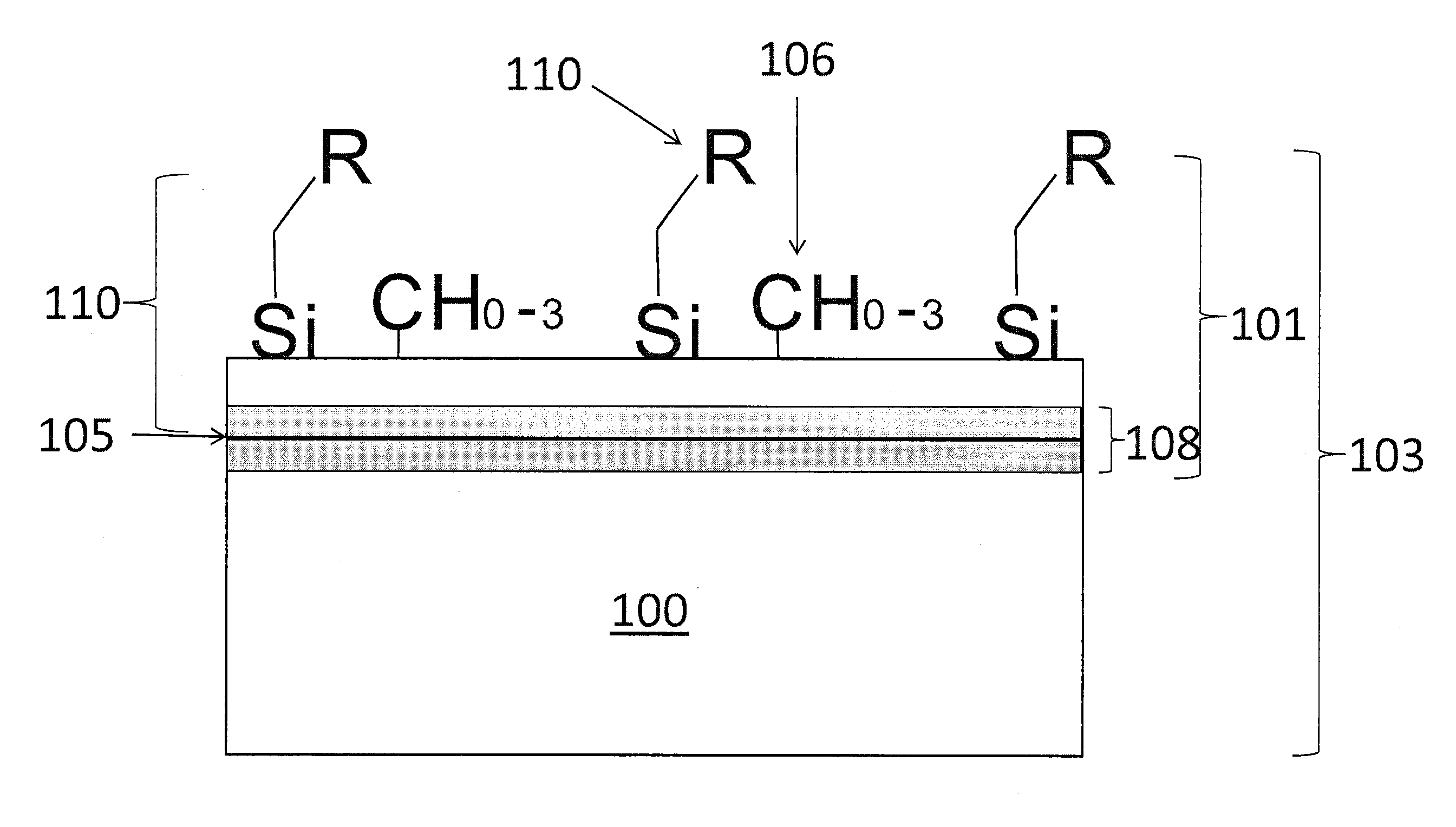
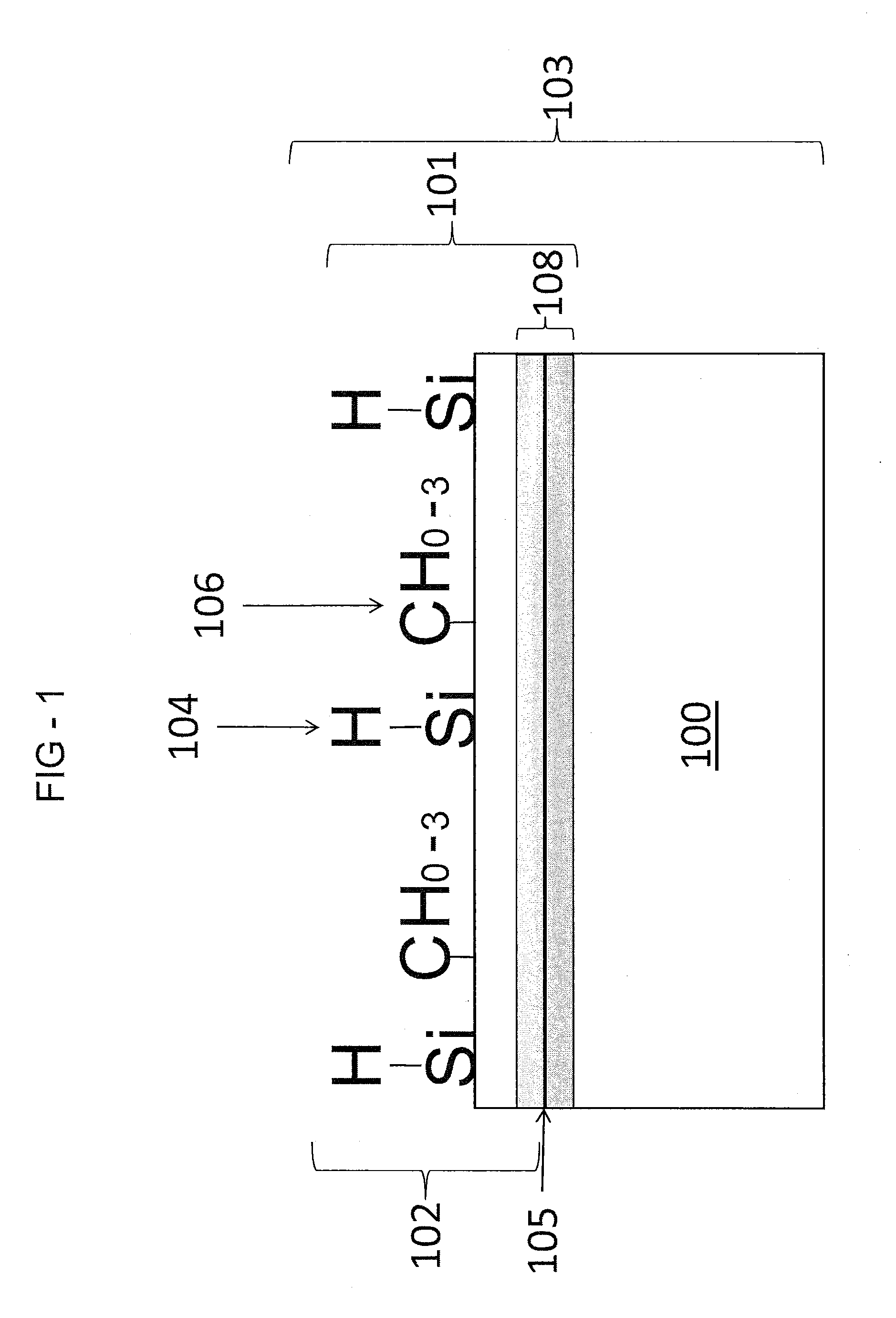
[0061]The first example included introducing dimethylsilane to the substrate 100 for 2 hours at 8 p.s.i.a. gas at 450° C. to form the layer 102. In the first example, the layer 102 was almost undetectable (i.e., very difficult to visually discern) on a mirror-polished 316 stainless steel coupon (slightly yellowed). Measurements showed water contact angle data prior to the deposition treatment at around 60°. After the deposition treatment with dimethylsilane, the contact angle increased to around 102°. Although the layer 102 was not visible, the data indicated an extremely thin deposition with a significant density of carbosilyl material on the layer 102 of the surface 105. The thickness of the layer 102 was estimated to be at about 100 Angstroms as available spectroscopic techniques were not sensitive enough to detect the coating.

example 2

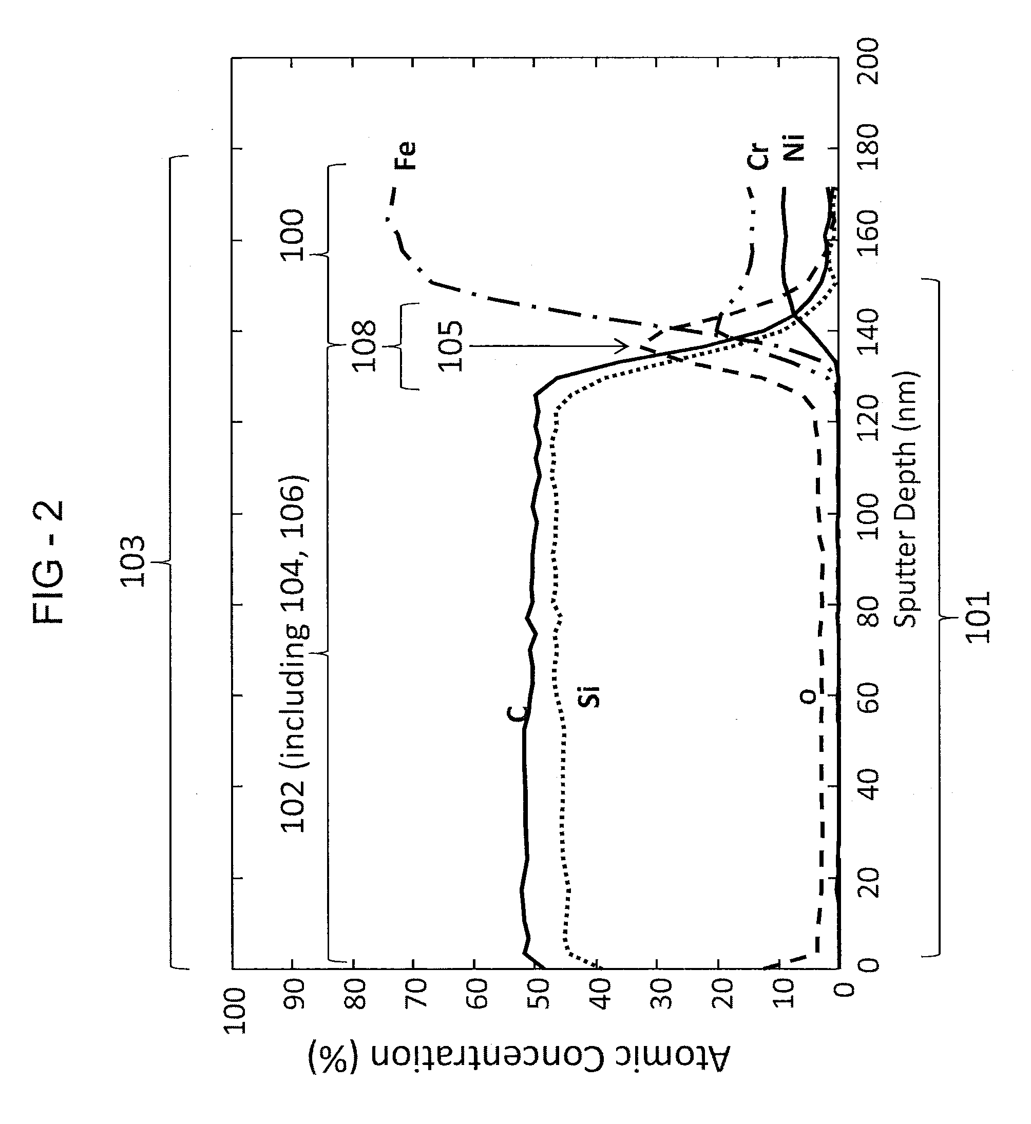
[0062]The second example included introducing dimethylsilane to the substrate 100 for 15 hours at 8 p.s.i.a. gas at 450° C. to form the layer 102. In the second example, the layer 102 had a visible luminescent rainbow array of colors. Measurements showed average deionized water contact angle data around 100°, for mirror-finished 316 stainless steel surfaces and polished silicon wafer surfaces. FT-IR indicated presence of C—H based upon a reading at 2950 cm−1, the presence of Si—C based upon a reading at 792 cm−1, and the presence of Si—H moieties based upon a reading at 2102 cm−1. The thickness of the layer 102 was determined by spectrometer to be about 800 Angstroms. Further measurements utilizing Auger Electron Spectroscopy were also performed. The measurements showed increased concentrations of Si and C atoms on the layer 102. The measurement further showed the concentration of Si and C atoms decreasing upon reaching the diffusion region 108 illustrated by the increase in concent...

example 3

[0063]The third example included introducing dimethylsilane to the substrate 100 for 15 hours at 8 p.s.i.a. gas at 450° C. to form the layer 102 and subsequently oxidizing the layer 102 of the substrate 100 with water in an inert gas for 2 hours at about 100 to 200 p.s.i.a. gas at 450° C. to form the oxidized layer 802. FT-IR data failed to reveal the significant presence of any functional moieties (Si—OH or Si—H) for surface modification chemistry. The resultant carboxysilane material revealed an improvement in hardness and wear resistance over the native carbosilane. The oxidized layer 802 had a contact angle on a Si wafer of 86.6°, and an increased presence of Si—O—Si groups.


PUM

PropertyMeasurementUnit
pressureaaaaaaaaaa
temperatureaaaaaaaaaa

Abstract

The present invention relates to a chemical vapor deposition coating, a chemical vapor deposition article, and a chemical vapor deposition method. The coating, article, and method involve thermal decomposition of dimethylsilane to achieve desired surface properties.

Description

PRIORITY[0001]The present application claims priority to and benefit of U.S. Provisional Patent Application No. 61 / 255,237, filed Oct. 27, 2009, and titled “DIMETHYLSILANE CHEMICAL VAPOR DEPOSITION COATING AND COATING PROCESS,” and U.S. Provisional Patent Application No. 61 / 267,228, filed Dec. 7, 2009, and titled “OXIDIZED VAPOR DEPOSITION COATING AND COATING PROCESS,” both of which are hereby incorporated by reference in their entirety.FIELD OF THE INVENTION[0002]The present disclosure is directed to chemical vapor deposition. More particularly, the disclosure is directed to chemical vapor deposition onto a substrate as a result of decomposition of dimethylsilane.BACKGROUND[0003]Often, surfaces of substrates do not include desired performance characteristics. The failure to include specific desired performance characteristics can result in surface degradation in certain environments, an inability to meet certain performance requirements, or combinations thereof. For example, in cer...

Claims


Application Information

Patent Timeline
Patent Type & Authority Applications(United States)
IPC IPC(8): C07F7/08B32B3/10C09D7/12C23C16/42
CPCB05D1/60B05D2202/15Y10T428/24802C23C16/325C23C16/56C23C8/10H01L21/0262
Inventor SMITH, DAVID A.MATTZELA, JAMES B.SILVIS, PAUL H.BARONE, GARY A.
Owner SILCOTEK CORP
Why Eureka
Try Eureka