Method for manufacturing semiconductor device

a manufacturing method and semiconductor technology, applied in the direction of semiconductor devices, basic electric elements, electrical appliances, etc., can solve the problems of difficult to sufficiently reduce electric resistance, unfavorable economic conditions, and need for a high-priced cmp process, so as to reduce internal stress, improve production efficiency, and reduce electric resistance

Active Publication Date: 2012-11-01
LONGITUDE LICENSING LTD
View PDF37 Cites 64 Cited by
  • Summary
  • Abstract
  • Description
  • Claims
  • Application Information

AI Technical Summary

Benefits of technology

[0014]According to an embodiment of the present invention, it is possible to freely determine the plan shapes and sizes (cross-sectional areas) of the through-electrode and the bump, and to continuously and integrally form the through-electrode and the bump. As a result, it is possible to reduce internal stress that causes a void due to stress migration of the conductive layer where the through-electrode is formed, and decrease electric resistance.
[0015]Further, it is possible to improve production efficiency because a film is formed faster in electrolytic plating than electroless plating.

Problems solved by technology

Particularly, since it is necessary to remove the plated metal (copper) on the chip surface when forming the through-electrode, a CMP process that is expensive is necessary, which is economically unfavorable.
Further, a barrier layer and a seed layer which have relatively large resistance are disposed between the through-electrode and the bump and the interface resistance is generated between the layers, such that it is difficult to sufficiently reduce electric resistance.
Further, the speed forming a film is low in electroless plating, which cannot be considered as a preferable method for the productivity.
As a result, it is possible to reduce internal stress that causes a void due to stress migration of the conductive layer where the through-electrode is formed, and decrease electric resistance.

Method used


Image

  • Method for manufacturing semiconductor device
  • Method for manufacturing semiconductor device
  • Method for manufacturing semiconductor device

Examples


first exemplary embodiment

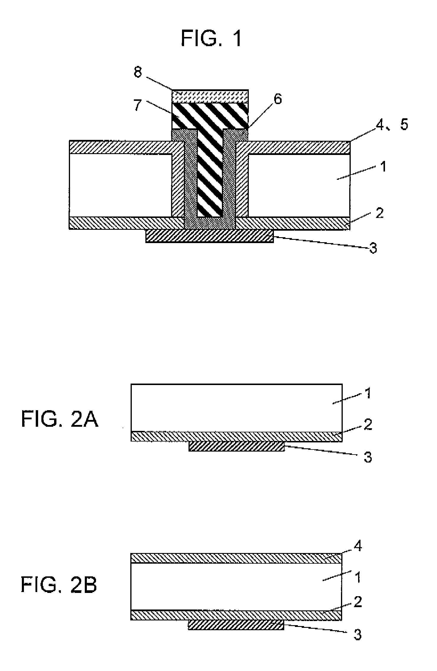
[0027]FIG. 1 shows the structure of a semiconductor device according to a first exemplary embodiment. An embodiment of an insulating layer liner type of a through-electrode is shown in the figure.

[0028]Meanwhile, a through-electrode is mainly described herein and other structures of the semiconductor device which do not largely relate to the present invention are not described.

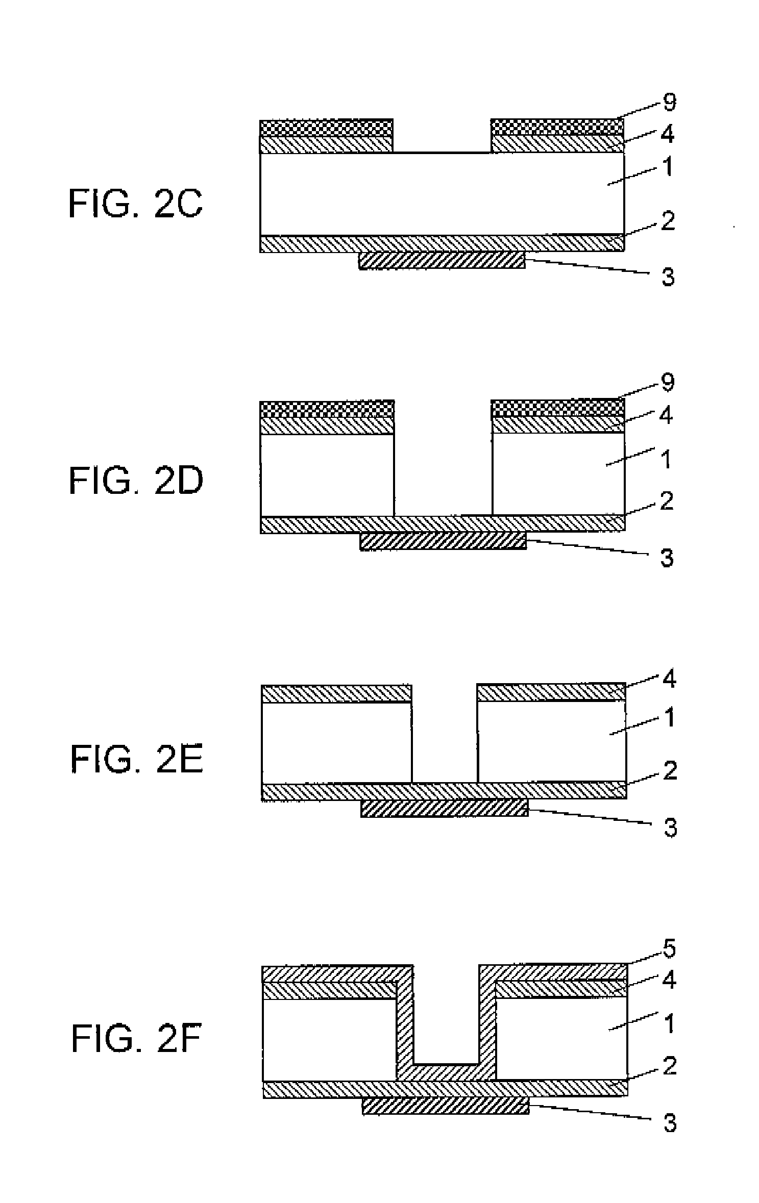
[0029]A semiconductor device of this exemplary embodiment includes a first insulating film 2 and a conductive layer 3 (referred to as a pad) which are disposed on one surface of a silicon substrate 1, a through-hole (Through silicon via, referred to as TSV) formed from the other surface of the silicon substrate 1, a second insulating film 4 and a third insulating film 5 which cover the other surface of the silicon substrate 1 and the side facing the TSV, and a barrier metal and a seed metal (totally referred to as a metal film 6), a first plated film 7, and a second plated film 8. The portion of the first plat...

second exemplary embodiment

[0076]Although the embodiment of an insulating layer liner type of a through-electrode having an insulating layer (third insulating film) on the side of the through-electrode is described in the first exemplary embodiment, the present invention is not limited thereto, and it may be possible to forming an insulative separating portion (insulating ring) around the through-electrode through from one surface to the other surface of a semiconductor substrate, in a region isolated from the through-electrode.

[0077]FIG. 6A is a cross-sectional view showing a through-electrode with an insulating ring and other structures of the semiconductor device which do not largely relate to the present invention are not shown, similar to FIG. 1.

[0078]A semiconductor device of the second exemplary embodiment includes a first insulating film 2 and a pad 3 which are disposed on one surface of a silicon substrate 1, a TSV formed from the other surface of the silicon substrate 1, a second insulating film 4 c...

modified embodiment

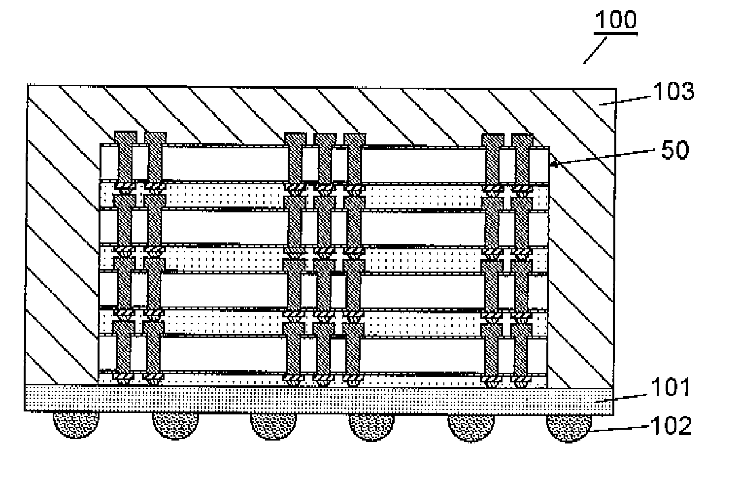
[0089]FIG. 8 and FIG. 9 show a modified example of a semiconductor device of the present invention.

[0090]FIG. 8 is a schematic cross-sectional view showing a stacking module 50 formed by stacking a plurality of semiconductor chips 51 of the present invention, with which a pad of one semiconductor chip is electrically connected to a bump portion in a bump-integrated through-electrode of another chip. The pad of the upper semiconductor chip is connected to the bump portion of the lower semiconductor chip via a connection terminal 52, such as BGA. Further, an insulating material 53 is under-filled between the chips, for insulation.

[0091]FIG. 9 shows a package 100 equipped with the stacking module 50 formed as described above on a circuit board 101, and sealed with mold resin 103. A plurality of wire layers (not shown) is formed in the circuit board 101 and stacked such that the width and the gap increase downward. Reference numeral ‘102’ indicates an external terminal, such as a BGA, w...


PUM


Abstract

In order to provide a semiconductor device that includes a conductive layer on one surface of a semiconductor substrate with an insulating layer therebetween, a bump on the other surface of the semiconductor substrate, and a through-electrode through the semiconductor substrate connecting the conductive layer with the bump, a through-hole is formed from the other surface of the semiconductor substrate to be connected to the conductive layer, a seed metal film is formed on the through-hole and the other surface, a photoresist is formed thereon, a mask layer is formed by processing the photoresist with a pattern larger than the through-hole, a plated film is grown by electrolytic plating so as to integrally form the through-electrode and a part of the bump.

Description

BACKGROUND OF THE INVENTION[0001]1. Field of the Invention[0002]The present invention relates to a method for manufacturing a semiconductor device including a through-electrode connecting conductive layers formed on one and the other surfaces of a semiconductor substrate, and a method for forming the through-electrode.[0003]2. Related Art[0004]As a technology for achieving additional high integration and high performance of semiconductor integrated circuits, there is a technology of stacking semiconductor chips with which a conductive layer provided on the main surface of the upper semiconductor chip is electrically connected to a conductive layer provided on the main surface of the lower semiconductor chip by a through-electrode formed in the upper semiconductor chip and in contact with the conductive layer of the upper semiconductor chip, and a bump between the through-electrode and the conductive layer of the lower semiconductor chip. Since the conductive layers are connected in ...

Claims


Application Information

Patent Timeline
Patent Type & Authority Applications(United States)
IPC IPC(8): H01L21/768
CPCH01L21/76898H01L21/2885H01L2924/15311H01L2224/73204H01L2224/32225H01L2224/32145H01L2224/16225H01L2224/16145H01L2225/06565H01L2225/06541H01L2225/06513H01L2225/06517H01L25/50H01L25/0657H01L2924/00
Inventor SAEKI, YOSHIHIROHOSHI, NOBUAKI
Owner LONGITUDE LICENSING LTD
Why Eureka
Try Eureka