Method of Manufacture of Sodium Doped CIGS/CIGSS Absorber Layers for High Efficiency Photovoltaic Devices

a photovoltaic device and absorber layer technology, applied in the field of manufacturing methods of thin film photovoltaic absorber materials, can solve the problems of limited supply of petrochemical fuel, many limitations remain to be resolved, and rapidly become a scarce resource, and achieve the effect of improving efficiency

Inactive Publication Date: 2012-11-29
CM MFG
View PDF13 Cites 10 Cited by
  • Summary
  • Abstract
  • Description
  • Claims
  • Application Information

AI Technical Summary

Benefits of technology

[0006]The invention relates generally to thin-film photovoltaic materials and manufacturing methods. More particularly, the invention provides a method for the manufacture of thin-film photo

Problems solved by technology

Unfortunately, the supply of petrochemical fuel is limited and essentially fixed based upon the amount available on the planet Earth.
Additionally, as more people use petroleum products in growing amounts, it is rapidly becoming a scarce resource.
Although solar energy is environmentally clean and has been successful to a point, many limitations remain to be resolved before it becomes widely used.
However, crystalline materials are often costly and difficult to make on a large scale.
Additionally, devices made from such crystalline materials often have low energy conversion efficiencies.
Similar limi

Method used


Image

  • Method of Manufacture of Sodium Doped CIGS/CIGSS Absorber Layers for High Efficiency Photovoltaic Devices
  • Method of Manufacture of Sodium Doped CIGS/CIGSS Absorber Layers for High Efficiency Photovoltaic Devices
  • Method of Manufacture of Sodium Doped CIGS/CIGSS Absorber Layers for High Efficiency Photovoltaic Devices

Examples


Embodiment Construction

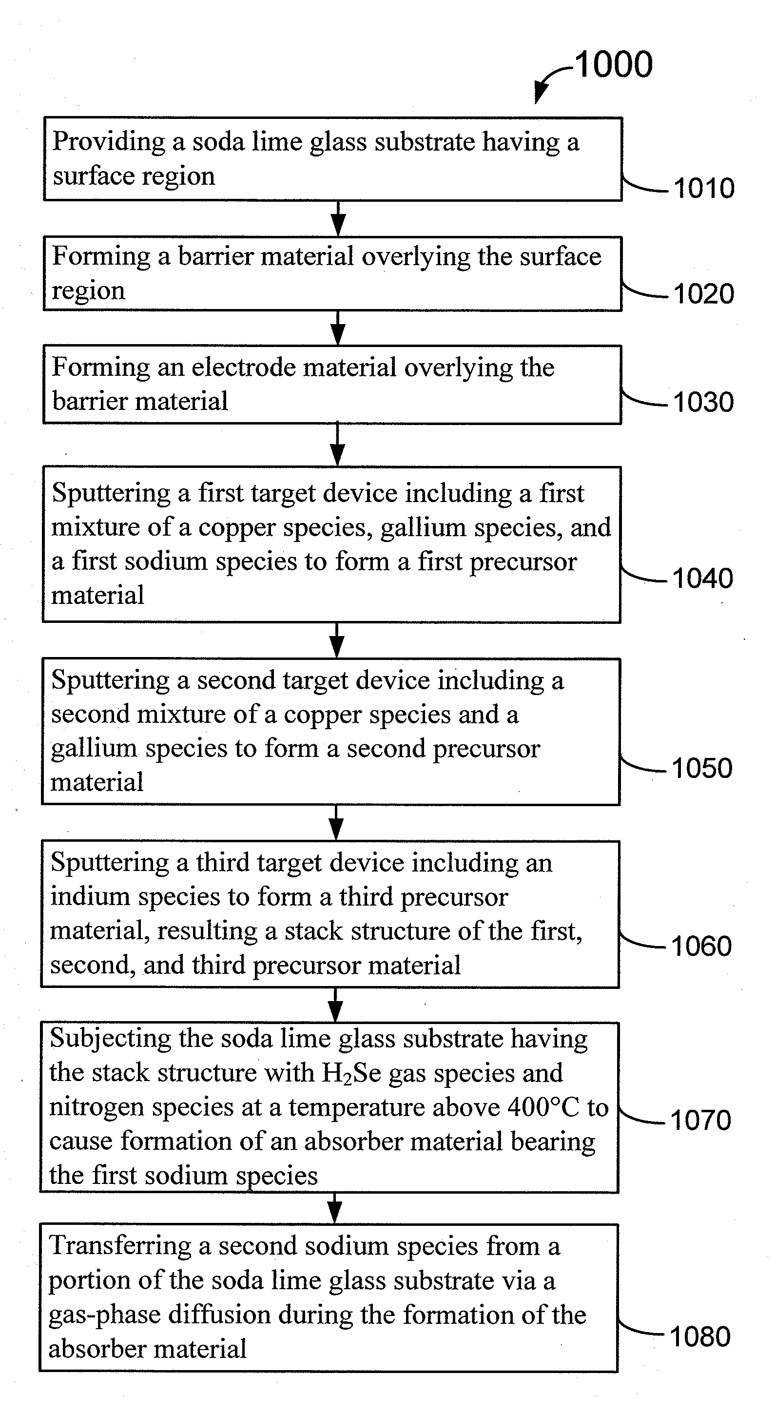
[0018]FIG. 1 is a flowchart illustrating a method of fabricating a thin-film photovoltaic absorber material. The method 1000 includes:

[0019]1. Process 1010 for providing a soda lime glass substrate having a surface;

[0020]2. Process 1020 for forming a barrier layer over the surface;

[0021]3. Process 1030 for forming an electrode over the barrier layer;

[0022]4. Process 1040 for sputtering a first mixture of a copper species, gallium species, and a first sodium species to form a first precursor material;

[0023]5. Process 1050 for sputtering a second mixture of a copper species and a gallium species to form a second precursor material;

[0024]6. Process 1060 for sputtering an indium species to form a third precursor material, resulting a stack structure;

[0025]7. Process 1070 for subjecting the soda lime glass substrate and stack structure to H2Se and nitrogen at a temperature above 400° C. to cause formation of absorber material; and

[0026]8. Process 1080 for transferring a second sodium spe...


PUM


Abstract

A method for processing a thin-film absorber material with enhanced photovoltaic efficiency includes forming a barrier layer on a soda lime glass substrate followed by formation of a stack structure of precursor layers. The method further includes subjecting the soda-lime glass substrate with the stack structure to a thermal treatment process with at least H2Se gas species at a temperature above 400° C. to cause formation of an absorber material. By positioning the substrates close together, during the process sodium from an adjoining substrate in the furnace also is incorporated into the absorber layer.

Description

CROSS-REFERENCE TO RELATED APPLICATION[0001]This application claims priority from U.S. Provisional Patent Application Ser. No. 61 / 523,802, filed Aug. 15, 2011, and entitled “Sodium Doped Absorber Layers for High Efficiency Photovoltaic Devices and Related Methods,” which is incorporated herein by reference.BACKGROUND OF THE INVENTION[0002]This invention relates to thin-film photovoltaic materials and manufacturing methods. More particularly, the invention provides a method for the manufacture of thin-film photovoltaic absorber materials which include sodium doping in the formation of a CIGS / CIGSS-based absorber material.[0003]From the beginning of time, mankind has been challenged to find ways of harnessing energy. Energy comes in the forms such as petrochemical, hydroelectric, nuclear, wind, biomass, solar, wood and coal. Over the past century, modern civilization has relied upon petrochemical energy as an important energy source. Petrochemical energy includes gas and oil. Unfortun...

Claims


Application Information

Patent Timeline
IPC IPC(8): H01L31/18
CPCH01L31/0322H01L31/0323H01L31/022441Y02E10/541H01L31/18H01L31/03923Y02P70/50
Inventor WIETING, ROBERT D.
Owner CM MFG
Why Eureka
Try Eureka