Semiconductor device and manufacturing method thereof

Active Publication Date: 2012-12-20
SEMICON ENERGY LAB CO LTD
View PDF1 Cites 144 Cited by
  • Summary
  • Abstract
  • Description
  • Claims
  • Application Information

AI Technical Summary

Benefits of technology

[0013]Further, in order to achieve a semiconductor device having higher performance, one object of the present invention is to provide a structure for improving on-state characteristics of the transistor (e.g., on-state current and field-effect mobility) and for achieving high-speed response and high-speed operation of the semiconductor device and a manufacturing method thereof.
[0014]Further, one object of the present invention is to provide a structure for suppressing generation of leakage current (parasitic channel) between a source electrode layer and a drain electrode layer of a transistor. To reduce leakage current of a transistor is important for obtaining a semiconductor device with low power consumption because leakage current of a transistor also affects power consumption.
[0015]A transistor is formed using stack of oxide semiconductor la

Problems solved by technology

If the threshold voltage of the transistor is negative, the transistor tends to be in a so-called normally-on state, in which current flows between the source electrode and the drain electrode even when the gate voltage is 0 V. For an LSI, a CPU or a memory, electric characteristics of transistors included in a circuit are significant and the electric characteristics aff

Method used


Image

  • Semiconductor device and manufacturing method thereof
  • Semiconductor device and manufacturing method thereof
  • Semiconductor device and manufacturing method thereof

Examples


embodiment 1

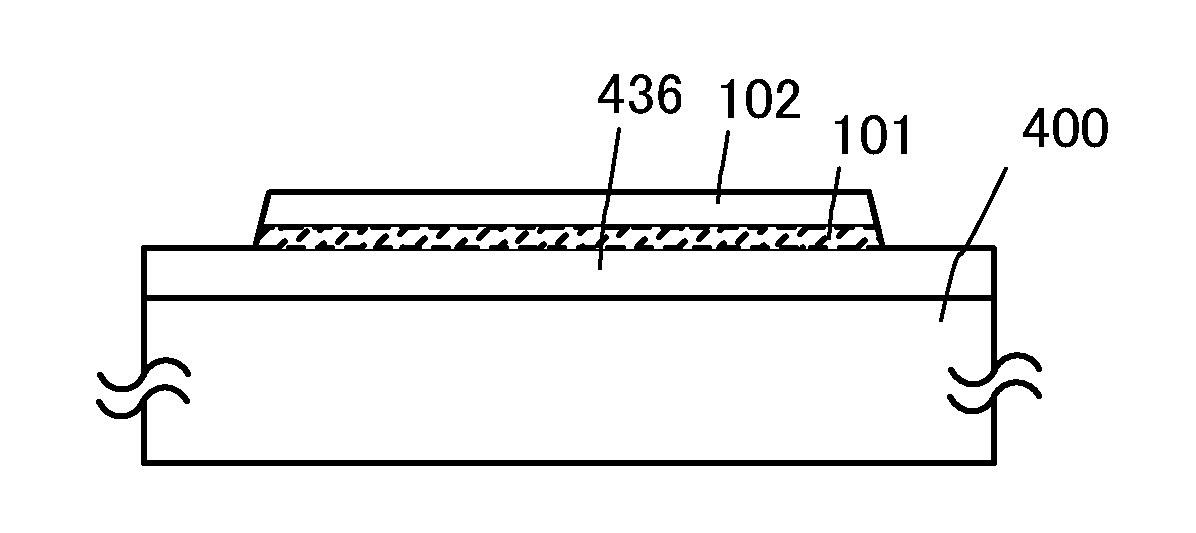
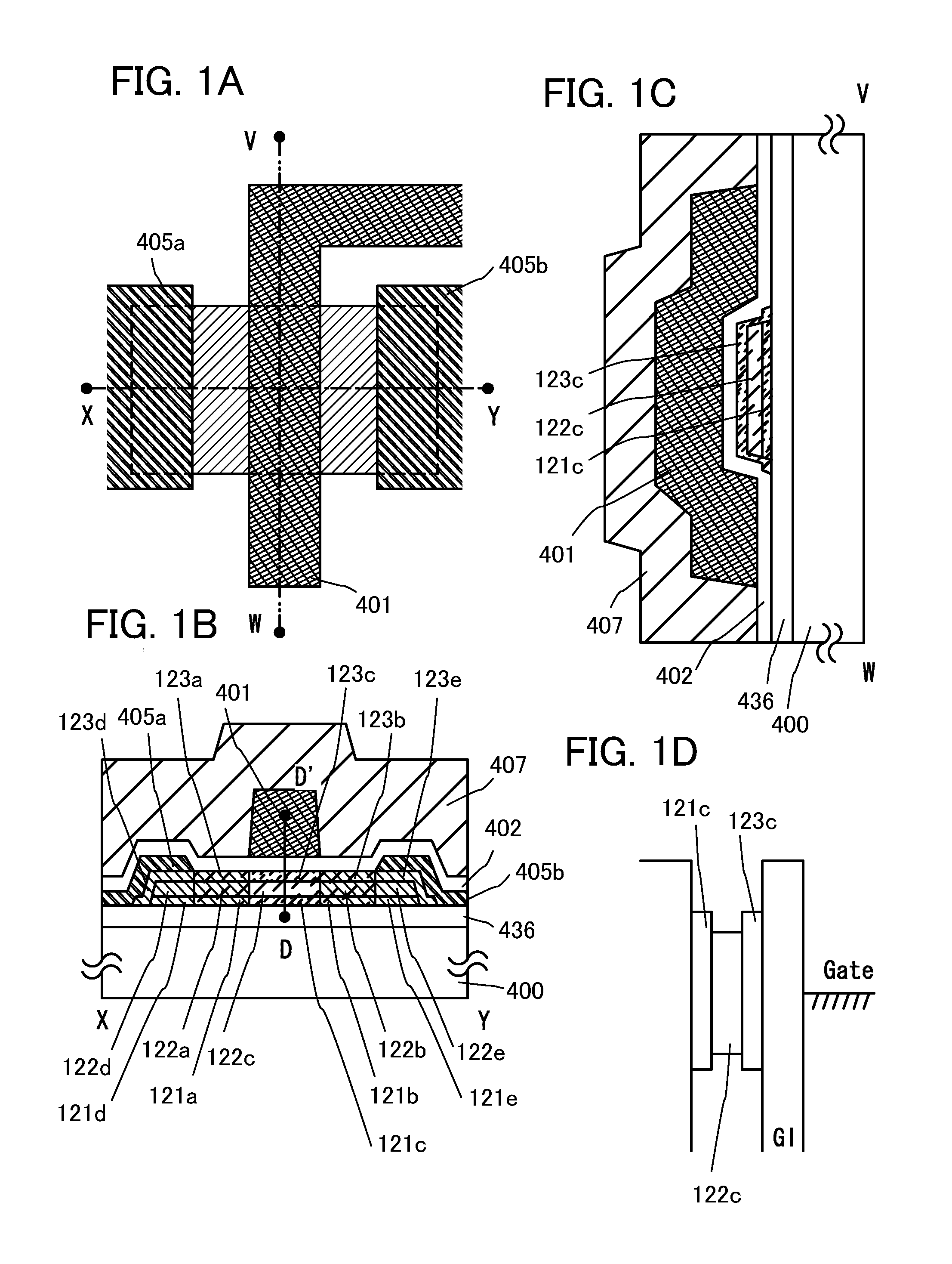
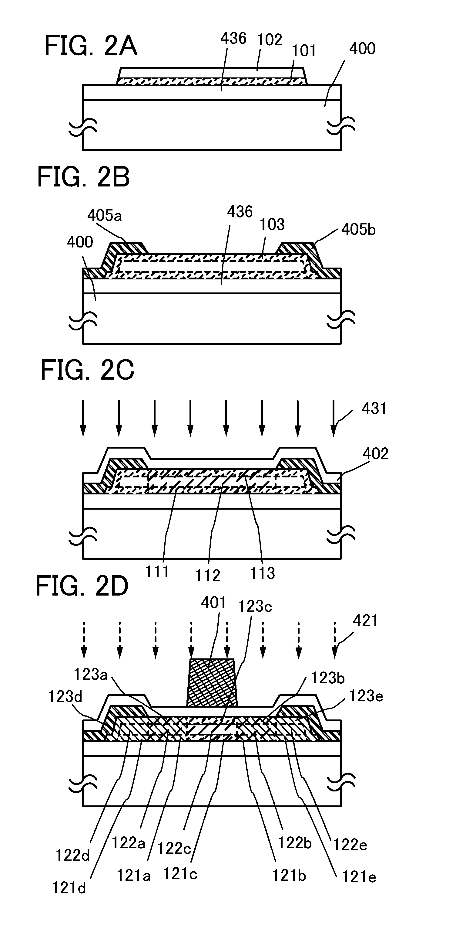
[0046]In this embodiment, one embodiment of a semiconductor device and one embodiment of a manufacturing method of the semiconductor device are described with reference to FIGS. 1A to 1D and FIGS. 2A to 2D. In this embodiment, a transistor including a stack of oxide semiconductor layers is shown as an example of the semiconductor device.

[0047]A transistor illustrated in FIGS. 1A to 1C is an example of a top-gate transistor. Note that although an example of a top-gate transistor is illustrated in FIGS. 1A to 1C, the present invention is not limited thereto and a bottom-gate transistor can also be manufactured, for example. Also, a dual-gate transistor can also be manufactured. In the dual-gate transistor, gate electrodes are provided over and below the stack of oxide semiconductor layers. FIG. 1A is a top view of the transistor, a cross section taken along the chain line X-Y of FIG. 1A corresponds to the cross-sectional view of FIG. 1B, and a cross section taken along the chain line ...

embodiment 2

[0115]In this embodiment, an example of a transistor which can be obtained by changing part of the process in Embodiment 1 is illustrated in FIGS. 3A to 3C. The same portions are denoted by the same reference numerals for simplicity. The transistor described in this embodiment is different from the transistor in Embodiment 1 just in part thereof; thus, the same portions are denoted by the same reference numerals for simplicity, and detailed description of the same portion is omitted here.

[0116]FIG. 3A illustrates a structure in which a region of the oxide insulating film 436 which does not overlap with the stack of oxide semiconductor layers is etched to be thin at the time of etching of the stack of oxide semiconductor layers. Etching is performed on up to part of the oxide insulating film so that etching residue such as residue of the first oxide semiconductor layer is removed, and generation of leakage current is suppressed. Further, in the structure of the transistor in FIG. 3A,...

embodiment 3

[0120]A semiconductor device having a display function (also referred to as display device) can be manufactured using the transistor described in Embodiment 1 or 2. Moreover, some or all of driver circuits which include transistors can be formed over a substrate where a pixel portion is formed, whereby a system-on-panel can be obtained.

[0121]In FIG. 4A, a sealant 4005 is provided so as to surround a pixel portion 4002 provided over a first substrate 4001, and the pixel portion 4002 is sealed by a second substrate 4006. In FIG. 4A, a signal line driver circuit 4003 and a scan line driver circuit 4004 which are each formed using a single crystal semiconductor film or a polycrystalline semiconductor film over a substrate prepared separately are mounted in regions that are different from the region surrounded by the sealant 4005 over the first substrate 4001. Various signals and potentials are supplied to the signal line driver circuit 4003, the scan line driver circuit 4004, or the pix...


PUM


Abstract

One object of the present invention is to provide a structure of a transistor including an oxide semiconductor in a channel formation region in which the threshold voltage of electric characteristics of the transistor can be positive, which is a so-called normally-off switching element, and a manufacturing method thereof. A second oxide semiconductor layer which has greater electron affinity and a smaller energy gap than a first oxide semiconductor layer is formed over the first oxide semiconductor layer. Further, a third oxide semiconductor layer is formed to cover side surfaces and a top surface of the second oxide semiconductor layer, that is, the third oxide semiconductor layer covers the second oxide semiconductor layer.

Description

BACKGROUND OF THE INVENTION[0001]1. Field of the Invention[0002]One embodiment of the present invention relates to a semiconductor device including a transistor or a semiconductor device including a circuit which is formed using a transistor. For example, one embodiment of the present invention relates to a semiconductor device including a transistor in which a channel formation region is formed using an oxide semiconductor or a semiconductor device including a circuit which is formed by using such a transistor. For example, the present invention relates to an electronic device which includes, as a component, a semiconductor integrated circuit including an LSI, a CPU, a power device mounted in a power circuit, a memory, a thyristor, a converter, an image sensor, or the like, or a light-emitting display device including a light-emitting element or an electro-optical device typified by a liquid crystal display panel.[0003]In this specification, a semiconductor device generally means a...

Claims


Application Information

Patent Timeline
IPC IPC(8): H01L29/78H01L21/336H05B44/00
CPCH01L29/267H01L29/7782H01L29/24H01L29/78696H01L29/045H01L29/7869H01L29/66742H01L29/78603H01L29/78609
Inventor YAMAZAKI, SHUNPEIHONDA, TATSUYA
Owner SEMICON ENERGY LAB CO LTD
Why Eureka
Try Eureka