Multi-step and asymmetrically shaped laser beam scribing

a laser beam and asymmetrical technology, applied in the field of semiconductor processing, can solve the problems of limited throughput, production issues or throughput limits, and the patterning resist may render the implementation cost prohibitive, and achieve the effect of increasing irradiance, reducing or increasing the width of the ker

Active Publication Date: 2012-12-20
APPLIED MATERIALS INC
View PDF4 Cites 48 Cited by
  • Summary
  • Abstract
  • Description
  • Claims
  • Application Information

AI Technical Summary

Benefits of technology

[0007]In an embodiment, a method of dicing a semiconductor substrate having a plurality of ICs includes receiving a masked semiconductor substrate, the mask covering and protecting ICs on the substrate. The masked substrate is ablated along streets between the ICs with a point on the substrate exposed to increasing irradiance. In one embodiment, at least a portion of the mask thickness in the street is ablated through exposure to electromagnetic radiation of first irradiance (optical intensity) to provide a patterned mask with gaps or trenches. At least a portion of a thin film device layer stack disposed below the mask is then ablated through exposure to electromagnetic radiation having second irradiance to expose regions of the substrate between the ICs. The ICs are then singulated into chips, for example by plasma etching through the exposed substrate following the trenches in the patterned mask.
[0008]In another embodiment, a system for dicing a semiconductor substrate includes a laser scribe module and a plasma etch chamber, integrated onto a same platform. The laser scribe module is to iteratively scribe the substrate and the plasma chamber is to etch through the substrate and singulate the IC chips. The laser scribe module may include one or more of a multiple lasers, a multi-pass controller, or a beam shaper to scribe the substrate via exposure to a plurality of optical intensities.
[0009]In another embodiment, a method of dicing a substrate having a plurality of ICs includes receiving a masked silicon substrate. The ICs include a copper bumped top surface having bumps surrounded by a passivation layer, such as polyimide (PI). Subsurface thin films below the bumps and passivation include a low-K interlayer dielectric (ILD) layer and a layer of copper interconnect, the entire set of layers comprising a device film layer stack. A femtosecond laser ablates, through irradiation, a predetermined pattern of trenches into the film layer stack by one or more sequential laser irradiation steps and into a thin film IC stack disposed below the mask with a second irradiance to expose a portion of a substrate and may further ablate into the same substrate such that there is sufficiently small amounts of residual film layer stack remaining on the substrate at the trench bottoms. The ablation leads with a first irradiance and follows with a second irradiance greater than, less than, or essentially equal to the first irradiance. The kerf width may additionally be reduced or increased with changing irradiance. A plasma etch is performed in a plasma etch chamber to additionally remove substrate material below the removed film layer stack to singulate individual ICs out of the single substrate. Any remaining mask material is then removed by a suitable method such as washing by solvent or dry plasma cleaning.

Problems solved by technology

For thin substrate singulation, such as <150 μms (μm) thick bulk silicon singulation, the conventional approaches have yielded only poor process quality.
Some of the challenges that may be faced when singulating die from thin substrates may include microcrack formation or delamination between different layers, chipping of inorganic dielectric layers, retention of strict kerf width control, or precise ablation depth control.
While plasma dicing has also been contemplated, a standard lithography operation for patterning resist may render implementation cost prohibitive.
Another limitation possibly hampering implementation of plasma dicing is that plasma processing of commonly encountered interconnect metals (e.g., copper) in dicing along streets can create production issues or throughput limits.
Finally, masking of the plasma dicing process may be problematic, depending on, inter alia, the thickness and top surface topography of the substrate, the selectivity of the plasma etch, and the materials present on the top surface of the substrate.

Method used


Image

  • Multi-step and asymmetrically shaped laser beam scribing
  • Multi-step and asymmetrically shaped laser beam scribing
  • Multi-step and asymmetrically shaped laser beam scribing

Examples


Embodiment Construction

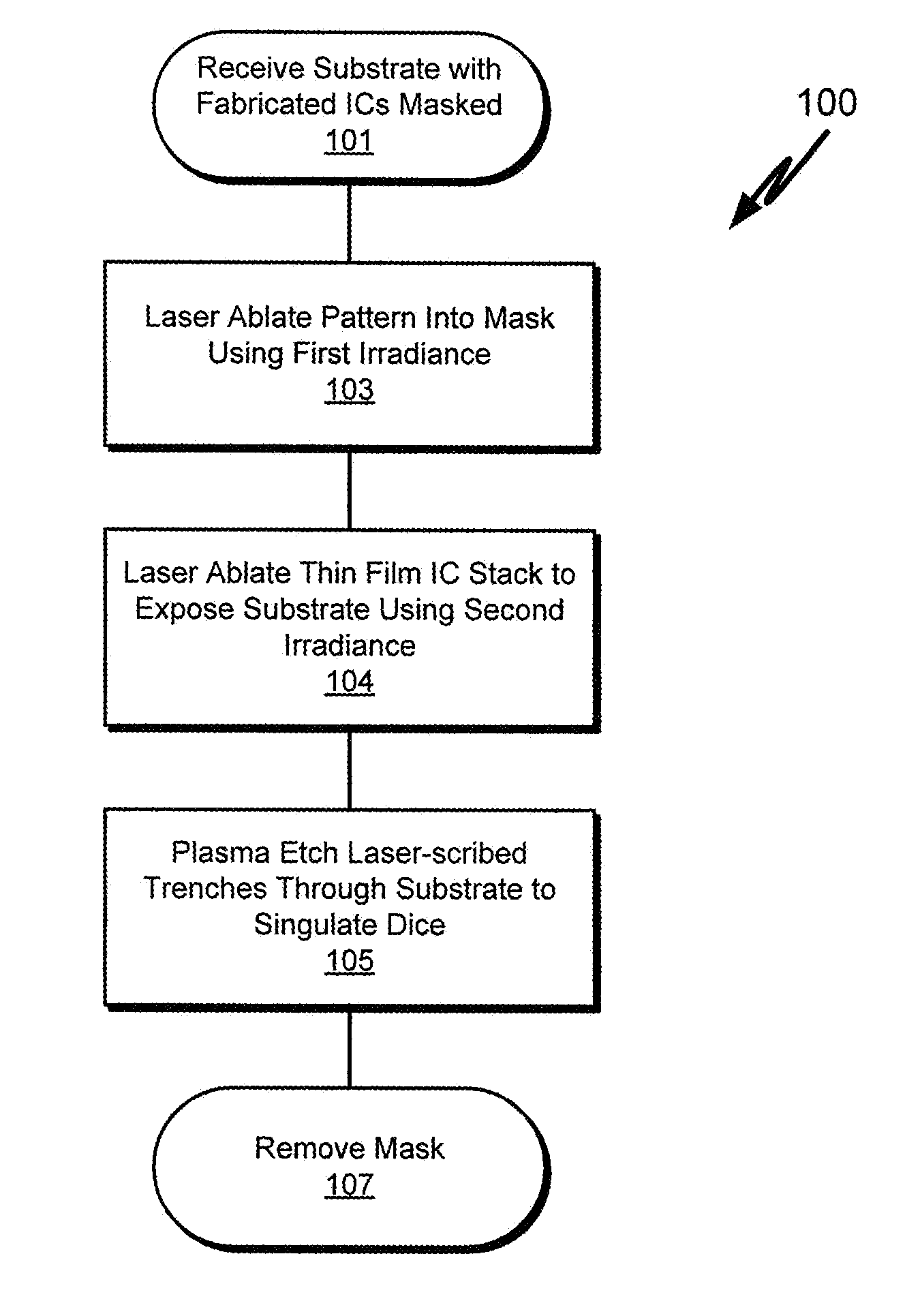
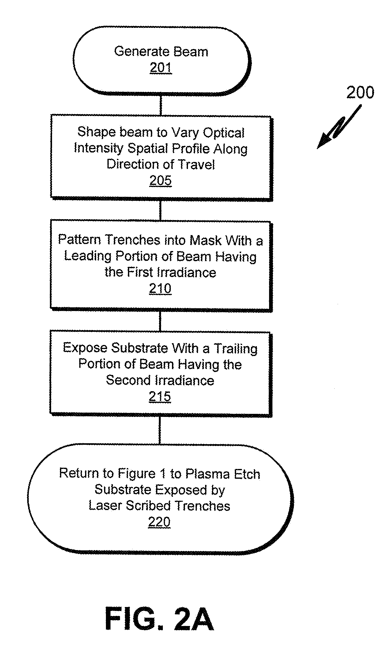
[0031]Methods of dicing substrates, each substrate having a plurality of ICs thereon, are described. In the following description, numerous specific details are set forth, such as femtosecond laser scribing and deep silicon plasma etching conditions in order to describe exemplary embodiments of the present invention. However, it will be apparent to one skilled in the art that embodiments of the present invention may be practiced without these specific details. In other instances, well-known aspects, such as IC fabrication, substrate thinning, taping, etc., are not described in detail to avoid unnecessarily obscuring embodiments of the present invention. Reference throughout this specification to “an embodiment” means that a particular feature, structure, material, or characteristic described in connection with the embodiment is included in at least one embodiment of the invention. Thus, the appearances of the phrase “in an embodiment” in various places throughout this specification ...


PUM

PropertyMeasurementUnit
diameteraaaaaaaaaa
pulse widthaaaaaaaaaa
thickaaaaaaaaaa

Abstract

Methods of dicing substrates by both laser scribing and plasma etching. A method includes laser ablating material layers, the ablating leading with a first irradiance and following with a second irradiance, lower than the first. Multiple passes of a beam adjusted to have different fluence level or multiple laser beams having various fluence levels may be utilized to ablate mask and IC layers to expose a substrate with the first fluence level and then clean off redeposited materials from the trench bottom with the second fluence level. A laser scribe apparatus employing a beam splitter may provide first and second beams of different fluence from a single laser.

Description

CROSS-REFERENCE TO RELATED APPLICATIONS[0001]This application is a continuation-in-part (CIP) of U.S. patent application Ser. No. 13 / 160,822, entitled “Multi-step and Asymmetrically Shaped Laser Beam Scribing,” and filed on Jun. 15, 2011, the entire contents of which are hereby incorporated by reference in its entirety for all purposes.TECHNICAL FIELD[0002]Embodiments of the present invention pertain to the field of semiconductor processing and, in particular, to methods for dicing substrates, each substrate having an integrated circuit (IC) thereon.BACKGROUND DESCRIPTION OF RELATED ART[0003]In semiconductor substrate processing, ICs are formed on a substrate (also referred to as a wafer), typically composed of silicon or other semiconductor material. In general, thin film layers of various materials which are either semiconducting, conducting or insulating are utilized to form the ICs. These materials are doped, deposited and etched using various well-known processes to simultaneou...

Claims


Application Information

Patent Timeline
Patent Type & Authority Applications(United States)
IPC IPC(8): H01L21/82H01L21/3065
CPCB23K26/0624B23K26/364B23K2103/42B23K2103/50B23K2103/172B23K26/40H01L21/3065H01L21/30655H01L21/67207H01L21/78B23K26/402
Inventor LEI, WEI-SHENGEATON, BRADYALAMANCHILI, MADHAVA RAOSINGH, SARAVJEETKUMARHOLDEN, JAMES M.
Owner APPLIED MATERIALS INC
Why Eureka
Try Eureka