Silicon epitaxial wafer, method for manufacturing the same, bonded soi wafer and method for manufacturing the same

a technology of silicon epitaxial wafers and bonded soi wafers, which is applied in the direction of basic electric elements, electrical apparatus, and semiconductor devices, can solve the problems of forming stripe-shaped steps, adverse effects on device characteristics, and none of the above documents, and achieves improved adhesiveness at the bonding interface, reduced defects due to bonding failure, and high quality.

Active Publication Date: 2012-12-27
SHIN-ETSU HANDOTAI CO LTD
View PDF3 Cites 10 Cited by
  • Summary
  • Abstract
  • Description
  • Claims
  • Application Information

AI Technical Summary

Benefits of technology

[0024]This inventive bonded SOI wafer has an SOT layer of a high dopant concentration of 1×10¹⁹ / cm3 or more, and also is a high quality wafer in which the adhesiveness at the bonding interface is improved and defects due to bonding failure are reduced.
[0026]Using the above silicon epitaxial wafer as the base wafer can ensure the bonded SOI wafer having the high dopant concentration layer (the epitaxial layer) just below the buried oxide film, and improved adhesiveness at the bonding interface of the bonded SOI wafer, thereby greatly reducing the defects of the bonded SOI wafer.
[0028]This inventive bonded SOI wafer has the high dopant concentration layer (the epitaxial layer) just below the buried oxide film, and also is a high quality wafer in which the adhesiveness at the bonding interface is improved and the defects due to bonding failure are reduced. In the bonded SOI wafer, the dopant can be phosphorus.
[0029]As described above, the present invention can provide the silicon epitaxial wafer having the epitaxial layer of a high dopant concentration of 1×10¹⁹ / cm3 or more, formed on the main surface of the silicon single crystal substrate. In the silicon epitaxial wafer, the stripe-shaped surface irregularities on the epitaxial layer is inhibited. The present invention can also provide the method for manufacturing the silicon epitaxial wafer. The present invention can further provide the high quality bonded SOI wafer having the high dopant concentration (a dopant concentration of 1×10¹⁹ / cm3 or more) SOI layer and having reduced defects, the bonded SOI wafer having the high dopant concentration layer (the epitaxial layer) just below the insulator film (the buried oxide film), and the method for manufacturing these wafers.

Problems solved by technology

As described above, there is the problem of forming stripe-shaped steps, caused by doping at high dopant concentrations, on the epitaxial layer surface to deteriorate its surface shape when the epitaxial layer is grown on the main surface of the silicon single crystal substrate.
None of the above documents, however, describes inhibiting the irregularities produced when the epitaxial layer is grown with doping at high dopant concentrations.
The presence of the irregularities has an adverse effect on device characteristics.
When a wafer referred to as an SOI (Silicon on Insulator) wafer is manufactured by bonding silicon epitaxial wafers having the irregularities together, there arises a problem in that adhesiveness at a bonding interface deteriorates and defects thereby occur.

Method used


Image

  • Silicon epitaxial wafer, method for manufacturing the same, bonded soi wafer and method for manufacturing the same
  • Silicon epitaxial wafer, method for manufacturing the same, bonded soi wafer and method for manufacturing the same
  • Silicon epitaxial wafer, method for manufacturing the same, bonded soi wafer and method for manufacturing the same

Examples


example 1

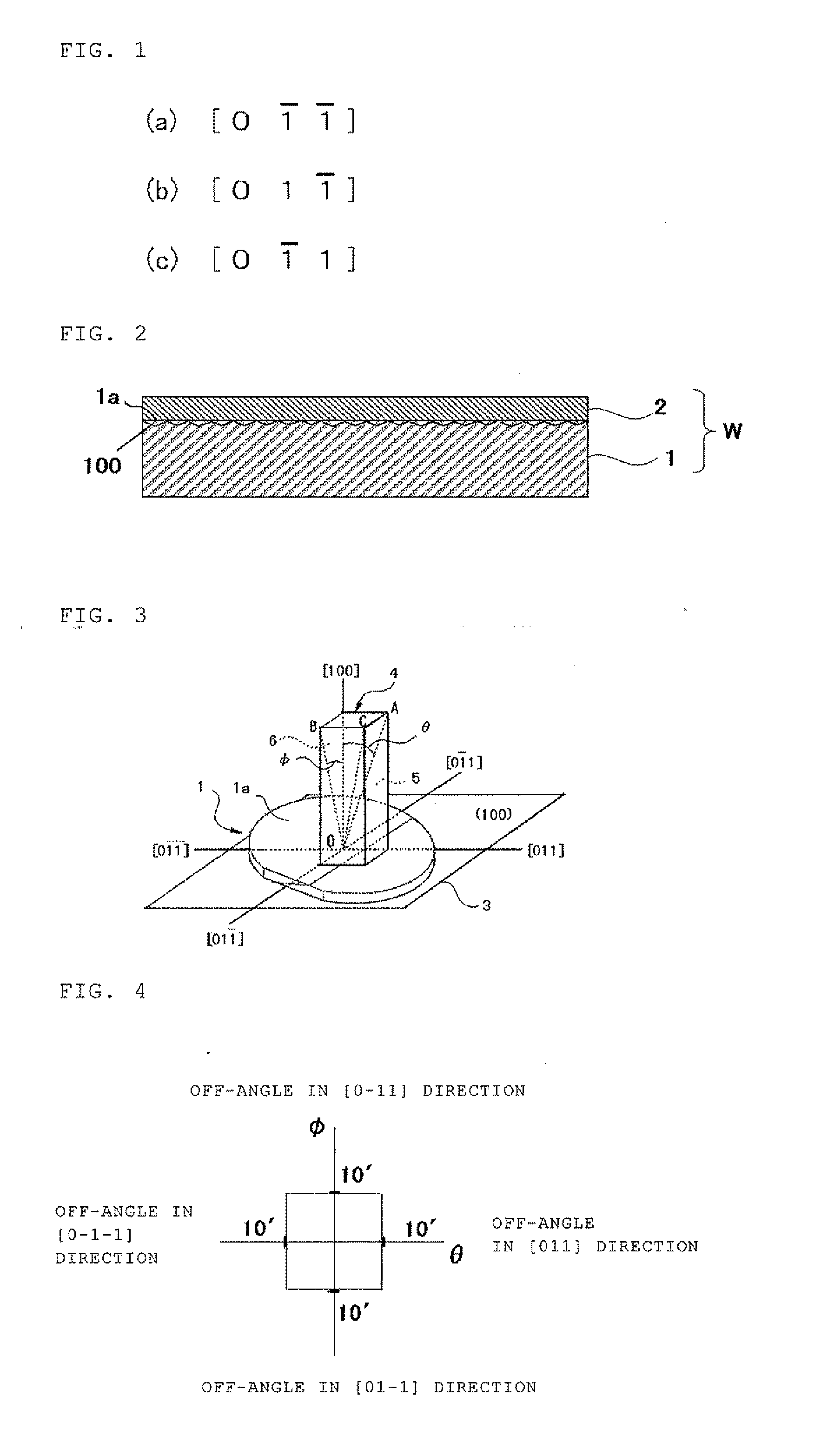
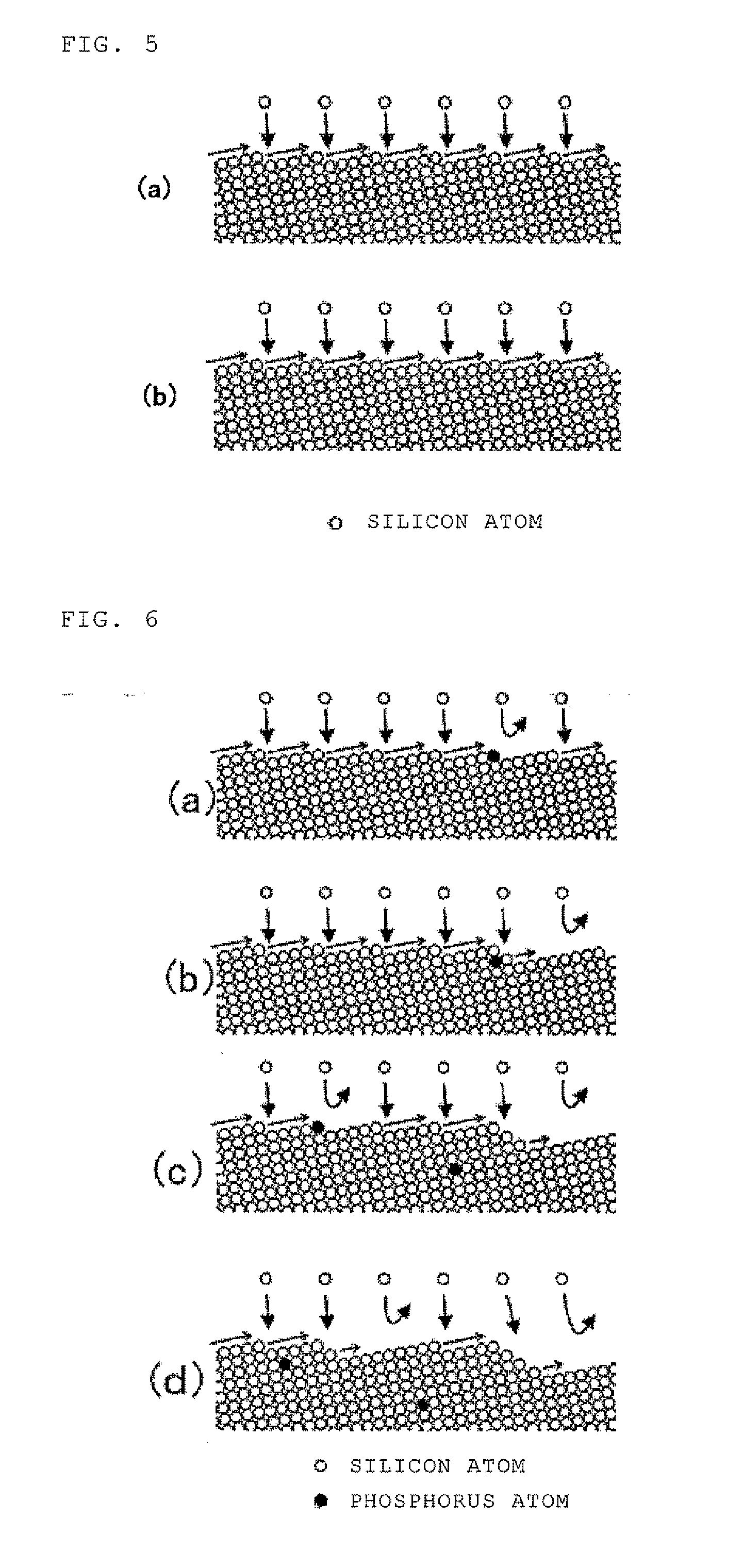
[0082]A 3 μm epitaxial layer was grown on the main surface of each of silicon single crystal substrates (a diameter of 300 mm) by vapor phase epitaxy at a growth temperature of 1080° C. while a phosphine (PH3) gas was introduced in conditions where the concentration of phosphorus in the epitaxial layer became 2×10¹⁹ / cm3. The main surface of each of the silicon single crystal substrates was tilted with respect to the [100] axis at an angle θ in the [011] direction from the (100) plane and at an angle Φ in the [01-1] direction from the (100) plane, where the angle θ satisfied 6′ (0.1°)≦θ≦9′ (0.15°) and the angle Φ was 1 minute. The material gas used herein was dichlorosilane.

example 2

[0091]The epitaxial wafer obtained in Example 1 was used as the bond wafer (the wafer for forming the SOI layer) to manufacture the bonded SOI wafer according to the method for manufacturing a bonded SOI wafer (using the ion implantation delamination method) shown in FIG. 8. The manufacture conditions will be described below.

(BOND WAFER): The epitaxial wafer manufactured in Example 1.

(BASE WAFER): A silicon single crystal substrate; a diameter of 300 mm; p-type, (100); 10 Ωcm.

(FORMATION OF OXIDE FILM): A 150 nm thermal oxide film formed on the surface of the bond wafer.

(ION IMPLANTATION): Hydrogen ions implanted through the oxide film on the surface of the bond wafer; 50 keV; 6×10¹⁶ / cm2.

(DELAMINATION HEAT TREATMENT): 500° C.; 30 minutes.

[0092]The bonding heat treatment was performed on the SOI wafer after delamination under an oxidizing atmosphere. After removing the oxide film from the surface, a flattening heat treatment was performed at 1200° C. under an Ar atmosphere for one hou...


PUM


Abstract

A silicon epitaxial wafer having a silicon epitaxial layer grown by vapor phase epitaxy on a main surface of a silicon single crystal substrate, wherein the main surface of the silicon single crystal substrate is tilted with respect to a [100] axis at an angle θ in a [011] direction or a [0-1-1] direction from a (100) plane and at an angle Φ in a [01-1] direction or a [0-11] direction from the (100) plane, the angle θ and the angle Φ are less than ten minutes, and a dopant concentration of the silicon epitaxial layer is equal to or more than 1×10¹⁹ / cm3. Even when an epitaxial layer having a dopant concentration of 1×10¹⁹ / cm3 or more is formed on the main surface of the silicon single crystal substrate, stripe-shaped surface irregularities on the epitaxial layer are inhibited.

Description

TECHNICAL FIELD[0001]The present invention relates to a silicon epitaxial wafer having a silicon epitaxial layer formed on a main surface of a silicon single crystal substrate and a method for manufacturing the silicon epitaxial wafer. The present invention also relates to a bonded SOI wafer and a method for manufacturing the bonded SOI wafer.BACKGROUND ART[0002]Silicon single crystal substrates for use in semiconductor substrates are manufactured by performing processes including slicing, chamfering, lapping, etching, and mirror-polishing on silicon single crystal ingots pulled, for example, by the CZ (Czochralski) method.[0003]A method for growing a silicon epitaxial layer by vapor phase epitaxy is also used to improve crystal quality at a surface portion of the silicon single crystal substrate. In this method, the silicon epitaxial layer is grown by supplying silicon raw material to a main surface of the silicon single crystal substrate under a high temperature condition.[0004]It...

Claims


Application Information

Patent Timeline
Patent Type & Authority Applications(United States)
IPC IPC(8): H01L29/06H01L21/20H01L21/762H01L29/02
CPCH01L21/02381H01L21/02433H01L29/78603H01L21/02576H01L21/76254H01L21/02532H01L21/0262
Inventor KATO, MASAHIROOKA, SATOSHIKOBAYASHI, NORIHIROISHIZUKA, TOHRUNOTO, NOBUHIKO
Owner SHIN-ETSU HANDOTAI CO LTD
Why Eureka
Try Eureka