

Mold for imprinting and production method thereof
a technology of imprinting molds and molds, applied in the field of imprinting molds, can solve the problems of increasing costs, limiting the possibility of only carrying out micron-order control, and requiring considerable time for forming patterns, and achieves fine patterns, reduced surface roughness of substrates, and high pattern precision.
- Summary
- Abstract
- Description
- Claims
- Application Information
AI Technical Summary
Benefits of technology
Problems solved by technology
Method used
Image

Examples
embodiment 1
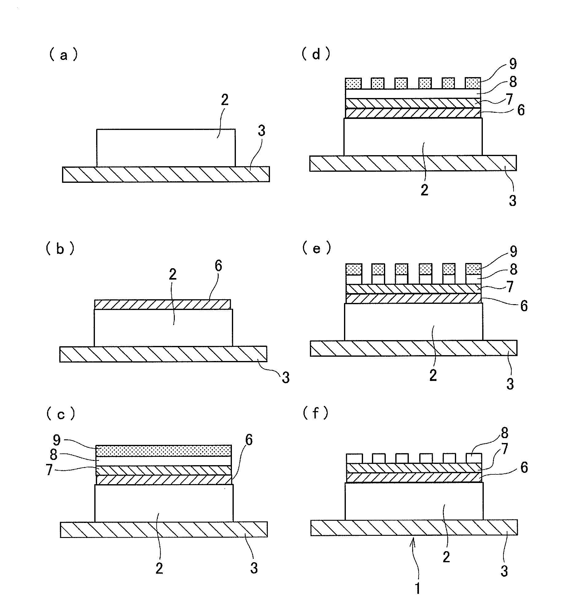
[0052]FIG. 1 is a view schematically showing a manufacturing process of an imprinting mold 1 according to this embodiment (also simply called a mold 1 hereafter). FIG. 1(a) shows a mold substrate 2, and FIG. 1(b) shows a state that a flattening layer 6 made of a flattening agent is formed on the mold substrate 2. Further, FIG. 1(c) shows a state that an adhesion layer 7, a fine pattern forming layer 8, and a resist layer 9 are laminated on the flattening layer 6 in this order, and FIG. 1(d) shows a state that the fine pattern is drawn / developed on the resist layer 9. Further, FIG. 1(e) shows a state that etching is applied to the fine pattern forming layer 8, and FIG. 1(f) shows a state that cleaning is performed after etching, to thereby complete the mold 1. As shown in FIG. 1(f), the imprinting mold can be obtained, in which the flattening layer 6 is provided on the mold substrate 2, and the adhesion layer 7 and the fine pattern forming layer 8 having a fine pattern formed thereon...
embodiment 2
[0089]According to embodiment 1, the substance having high transparency was used as the flattening agent. However, according to this embodiment, the substance having opaqueness is used as the flattening agent. Thus, the focus during pattern drawing is prevented from being adjusted to the rough surface of the substrate, even if the opaque layer is not used on the fine pattern forming layer 8. Namely, since the flattening agent itself is opaque, the focus can be surely adjusted to the surface of the flattened layer 6 during pattern drawing. Therefore, the resist layer 9 having the fine pattern can also be directly formed on the flattening layer 6. Note that when the surface of the mold substrate 2 has a certain degree of flatness like the silicon wafer, the imprinting mold can be formed by forming the resist layer 9 having the fine pattern directly on the flattening layer 6.
[0090]The flattening agent added with pigment additive can be given for example as the flattening agent having o...
example 1
[0092]The present invention will be more specifically described next, by showing examples.
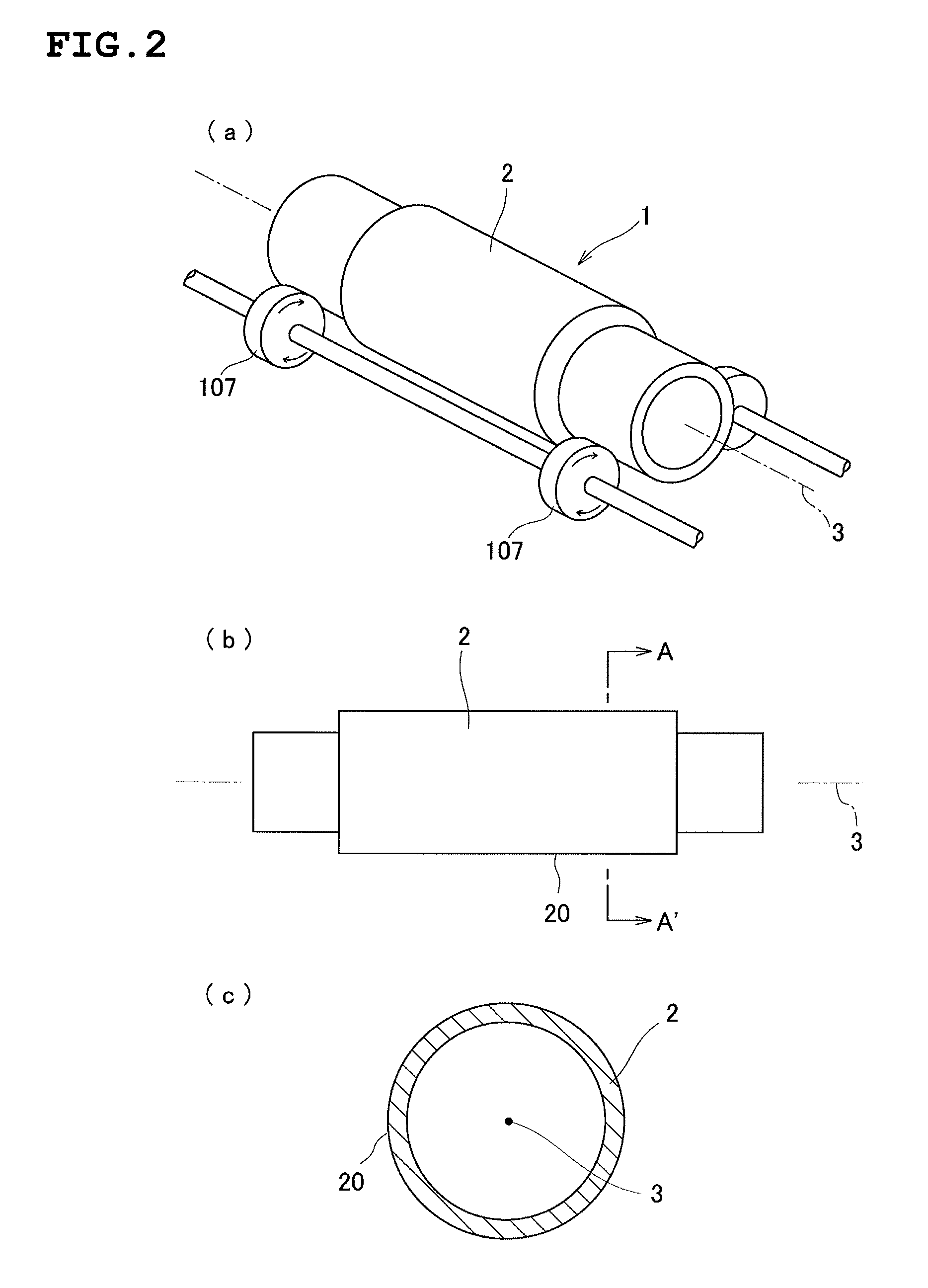
[0093]A stainless cylindrical hollow mold substrate 2 (SUS304, having diameter of 100 nm, namely having a radius of 50 mm, out of which diameter of a hollow portion: 84 mm, and distance between mold end faces: 300 mm) was prepared.
[0094]Next, the flattening agent was prepared. Solution obtained by dissolving 20% of polysilazane into dibutyl ether, was used as the flattening agent. A vessel of the flattening agent having the polysilazane ether therein, was disposed in a lower part of the mold substrate 2.
[0095]Thereafter, the mold substrate 2 is brought into contact with the polysilazane solution. At this time, a part of the outer peripheral surface 20 of the mold is dipped into the flattening agent in a depth of 0.3 mm or less from a liquid face of the flattening agent.
[0096]In this state, the mold is rotated at a rotation speed of 32 rotations / minute by the separately provided rotary shaft 3, ...
PUM
| Property | Measurement | Unit |
|---|---|---|
| thickness | aaaaa | aaaaa |
| thickness | aaaaa | aaaaa |
| thickness | aaaaa | aaaaa |
Abstract
Description
Claims
Application Information