Plasma processing apparatus
a technology of processing apparatus and plasma, which is applied in the direction of chemical vapor deposition coating, electric discharge tube, coating, etc., can solve the problems of affecting the exhaustion of reactive products that hinder the process, requiring a high input power for plasma generation, and may not be applicable in the method
- Summary
- Abstract
- Description
- Claims
- Application Information
AI Technical Summary
Benefits of technology
Problems solved by technology
Method used
Image
Examples
first embodiment
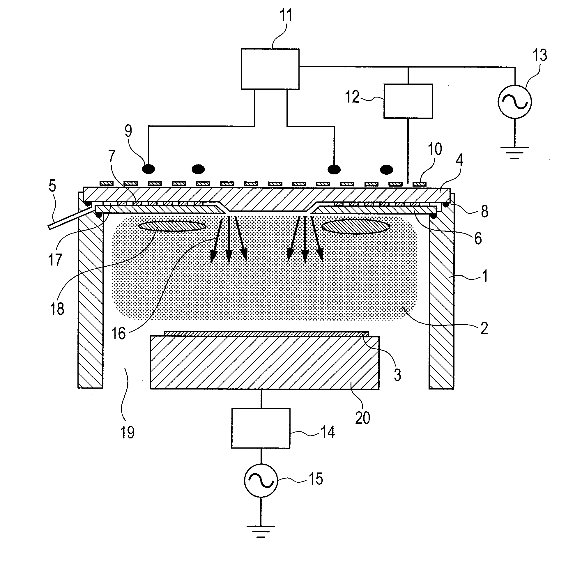
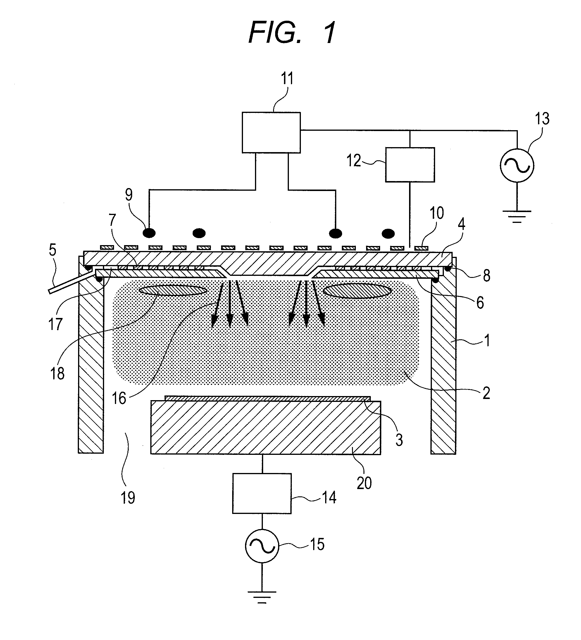
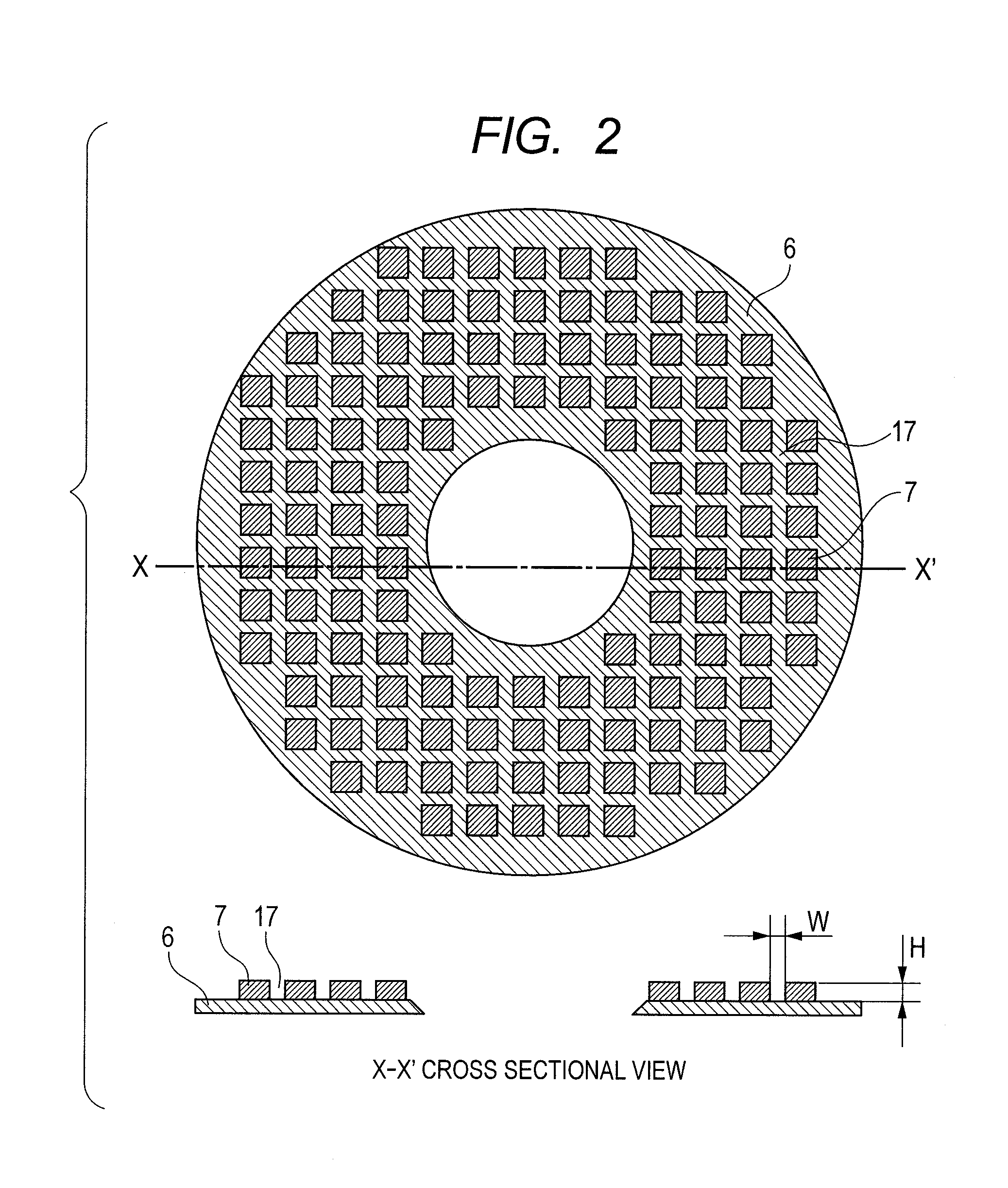
[0027]A first embodiment of the present invention will be described with reference to FIG. 1. FIG. 1 is a schematic diagram of a plasma processing apparatus according to the first embodiment. A sample (an object to be processed) 3, such as a semiconductor device wafer or a liquid crystal display substrate, is placed on a sample holding electrode (sample holder) 20. The sample holder has an electrostatic adsorption function and is provided in a process chamber 1. A radio-frequency of several tens of MHz or less is applied from a radio-frequency power supply 15 to the sample 3 through a matching box 14, to control the ion energy from a plasma 2 incident on the sample 3. In this embodiment, a semiconductor device wafer with a diameter of 300 mm is used as the sample 3, and a power supply with a frequency of 800 kHz is used as the radio-frequency power supply 15. The side wall of the process chamber 1 is formed by thermally spraying ceramic onto aluminum base metal. A dielectric vacuum ...
second embodiment
[0037]A second embodiment according to the present invention will be described with reference to FIG. 3. It is to be noted that the items described in the first embodiment, but not described in the second embodiment, can also be applied to this embodiment unless special circumstances exist. FIG. 3 is a detailed view of a gas guide plate in the plasma processing apparatus according to this embodiment. The upper diagram is a top view, the middle diagram is an A-A′ cross-sectional view, and the lower diagram is a B-B′ cross-sectional view. In this embodiment, the part including the dielectric vacuum window 4, the gas guide plate 6, and the dielectrics 7 in the first embodiment is replaced by the configuration of the dielectric vacuum window 4, the gas guide plate 6, and the dielectrics 7 shown in FIG. 3. The gas guide plate 6 is made from quartz. Plural gas inlet holes 25 with a diameter of about 0.5 mm are formed in the center of the gas guide plate 6 to introduce gas therefrom. The d...
third embodiment
[0040]A third embodiment according to the present invention will be described with reference to FIG. 4. It is to be noted that the items described in the first or second embodiment, but not described in the third embodiment, can also be applied to this embodiment unless special circumstances exist. FIG. 4 is a cross-sectional view showing the details of a gas guide plate in the plasma processing apparatus according to the third embodiment. In this embodiment, the high dielectric 7 used in the first and second embodiments is replaced by a conductor 32 covered by a dielectric 70. When using the conductors 32 in place of the high dielectrics 7, it is also effective in directing the electric field vectors to the conductors 32 to reduce the electric field strength of the gas flow path 17, similarly to the case of the dielectrics 7. In other words, the effect of reducing the electric field of the gas flow path 17 can also be obtained by the conductors 32. However, the reactive gas also fl...
PUM
| Property | Measurement | Unit |
|---|---|---|
| Shape | aaaaa | aaaaa |
| Electrical conductor | aaaaa | aaaaa |
| Height | aaaaa | aaaaa |
Abstract
Description
Claims
Application Information


